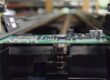


IPC-610, also known as IPC-A-610, is a widely recognized standard published by the Institute for Printed Circuits (IPC) that establishes the acceptability criteria for the assembly of electronic assemblies, including printed circuit boards (PCBs). It provides guidelines and requirements for PCB manufacturing and assembly processes, as well as the inspection and acceptance of finished electronic assemblies.
The IPC-610 standard covers a wide range of criteria related to the quality and reliability of PCBs and PCB assemblies. It defines various classes of electronic assemblies based on their application and provides specific criteria for each class. The classes include:
- Class 1: General Electronic Products – These are typically consumer electronic products where performance and extended life are not critical.
- Class 2: Dedicated Service Electronic Products – These products require continued performance and extended life but not to the level of Class 3.
- Class 3: High-Performance Electronic Products – These are mission-critical products, such as aerospace and medical devices, where safety and performance are paramount.
The IPC-610 standard covers a wide range of topics related to PCB and PCB assembly, including:
- Component Placement: It defines the acceptable alignment, spacing, and orientation of components on the PCB to ensure proper functionality and reliability.
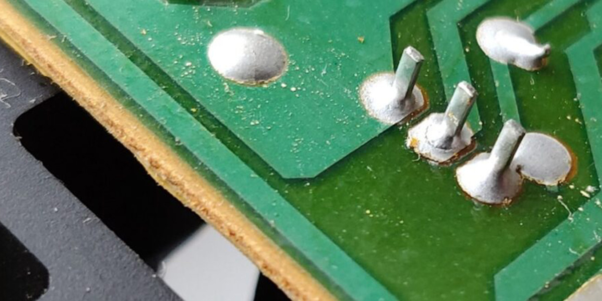
- Soldering: The standard provides guidelines for soldering processes, including the acceptable amount of solder, fillet shape, and wetting of solder joints.
- Soldering Defects: It outlines various soldering defects that can occur during the assembly process, such as solder bridges, cold solder joints, and insufficient solder.
- Surface Mount Technology (SMT): The standard covers guidelines for SMT processes, including solder paste application, component placement, and reflow soldering.
- Through-Hole Technology (THT): It provides criteria for through-hole component installation, including lead forming, hole diameter, and soldering techniques.
- Cleaning and Coating: The standard addresses the cleaning and coating of PCB assemblies, including the acceptable residues, coating thickness, and conformal coating applications.
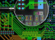
- Inspection and Acceptance: It specifies the criteria for visual inspection and acceptance of PCB assemblies, including acceptable levels of defects, such as solder voids, component damage, and PCB warpage.
By adhering to the IPC-610 standard, PCB manufacturers and assemblers can ensure that their products meet the required quality and reliability standards. Compliance with IPC-610 helps to minimize the risk of defects, improve product performance, and enhance customer satisfaction. It is widely used in the electronics industry as a benchmark for PCB assembly quality.
Certainly! Here are some examples of common soldering defects that can occur during the PCB assembly process:
- Solder Bridging: This defect occurs when solder unintentionally connects two adjacent electrical connections, creating a short circuit. It can happen when excessive solder paste or improper reflow conditions cause the solder to spread across the gaps between the pads or pins.
- Insufficient Solder: Insufficient solder occurs when there is an inadequate amount of solder to form a reliable joint. It can happen due to factors such as improper stencil design, insufficient solder paste deposition, or insufficient reflow conditions. Insufficient solder can lead to poor electrical conductivity and weak mechanical joints.
- Solder Balling: Solder balling refers to the formation of small spheres of solder on the PCB surface or between adjacent pads. It often occurs due to excessive solder paste deposition or improper reflow conditions. Solder balls can cause short circuits, especially when they bridge adjacent pads or come into contact with conductive traces.
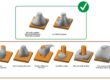
- Tombstoning: Tombstoning occurs when a surface-mounted component partially lifts off from one end during the reflow process, creating an uneven solder joint. It typically happens when there is a significant difference in thermal characteristics between the two pads of a component or uneven heating during reflow. Tombstoning can result in poor electrical contact and compromised mechanical stability.
- Cold Solder Joint: A cold solder joint is a defect where the solder hasn’t properly melted and wetted the surfaces being joined. It can occur due to insufficient heat during soldering or poor soldering technique. Cold solder joints can lead to weak connections, poor electrical conductivity, and increased susceptibility to mechanical stress.
- Solder Voids: Solder voids are small air pockets or gaps within the solder joint. They can occur due to various factors, including inadequate solder paste deposition, improper reflow conditions, or the presence of trapped gases. While small voids are generally acceptable, excessive voiding can affect thermal conductivity and mechanical strength.
- Excessive Solder: Excessive solder refers to an overabundance of solder that results in an irregular or bulky joint. It can occur due to excessive solder paste deposition, improper component placement, or excessive reflow conditions. Excessive solder can lead to solder bridging, poor electrical contact, and difficulty in fitting the assembled PCB into its intended enclosure.
These are just a few examples of soldering defects that can occur during PCB assembly. Adhering to proper soldering techniques, following the recommended guidelines for solder paste deposition and reflow, and conducting thorough inspection and quality control procedures can help minimize these defects and ensure the reliability of the assembled PCBs.