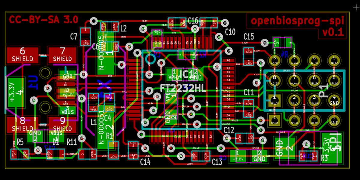
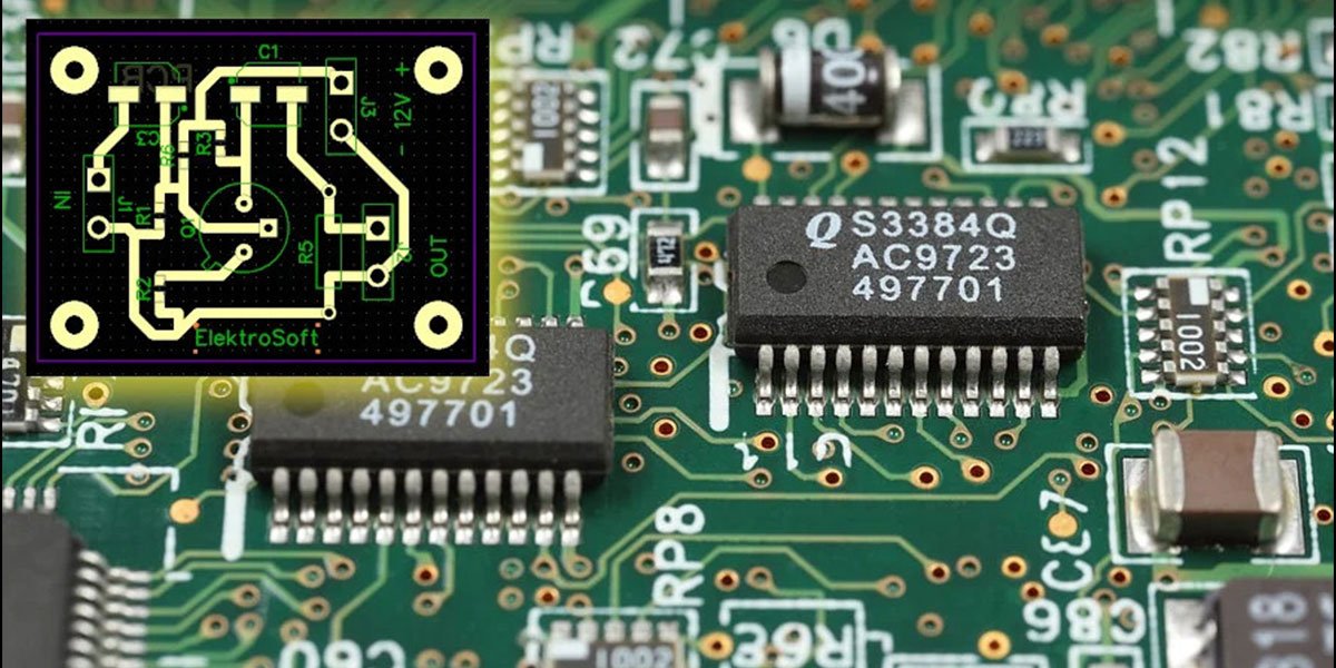
The term “Gerber file” is commonly used in the field of electronic circuit board design and fabrication. It refers to a standard file format that contains the information necessary for manufacturing printed circuit boards (PCBs).
Gerber files are generated by electronic design automation (EDA) software, such as PCB layout tools, and they provide a detailed description of the PCB’s copper layers, solder mask, and silkscreen layers. These files are named after the Gerber Scientific Instrument Company, which developed the format in the 1980s.
Here are the main components of a Gerber file:
- Copper Layers: A Gerber file includes separate layers for each copper conductor on the PCB. These layers represent the traces, pads, and other copper features that form the electrical connections of the circuit. Each layer is represented by a different Gerber file.
- Solder Mask Layer: The solder mask layer defines the areas on the PCB where solder should not be applied during the assembly process. It helps prevent solder bridges and ensures proper soldering of components.
- Silkscreen Layer: The silkscreen layer contains markings, text, and symbols that are printed on the PCB’s surface. These markings provide information such as component reference designators, part numbers, logos, and assembly instructions.
- Drill Data: In addition to the copper layers, a Gerber file includes drill data that specifies the locations and sizes of the holes to be drilled on the PCB. This information is crucial for creating the holes necessary for component mounting and interconnecting layers.

Gerber files are the industry standard for PCB manufacturing because they can be easily interpreted by PCB fabrication facilities and are compatible with various manufacturing processes. Once the Gerber files are generated, they are typically sent to a PCB manufacturer for production. The manufacturer uses the Gerber files to create the necessary tooling, such as photomasks and drilling templates, to fabricate the PCB according to the design specifications.
It’s worth noting that Gerber files alone may not provide a complete representation of the PCB design, as they do not include information about components, nets, or electrical connections. Therefore, in addition to Gerber files, other files such as Bill of Materials (BOM) and assembly drawings are often required for a comprehensive PCB fabrication and assembly process.
Certainly! In addition to the basic components I mentioned earlier, here are some additional details about Gerber files and their usage in the PCB design and manufacturing process:
1. File Extensions: Gerber files typically have specific file extensions to indicate their purpose and content. Some common Gerber file extensions include:
- GTL or .GBL: Top copper layer.
- GTS or .GBS: Bottom copper layer.
- GTO or .GBO: Top or bottom silkscreen layer.
- GTP or .GBP: Top or bottom solder mask layer.
- GKO: Board outline layer.
- TXT: Drill file containing drill hole locations and sizes.
2. Aperture Definitions: Gerber files use aperture definitions to specify the shapes and sizes of the features on the PCB. The aperture definitions define the tooling needed to create the various elements of the PCB, such as pads, tracks, and cutouts. Aperture definitions are typically included in a separate file or within the Gerber file itself.

3. Units and Coordinate System: Gerber files use a defined coordinate system to accurately represent the PCB layout. The units of measurement, such as millimeters or inches, are specified in the Gerber file. The origin point and the direction of positive coordinates are also defined to ensure proper alignment and positioning of the PCB features.
4. Gerber X2: The Gerber X2 format is an extension to the original Gerber format that includes additional information, such as component and net data, directly within the Gerber files. This enhanced format aims to improve the accuracy and efficiency of the PCB fabrication and assembly process by consolidating more information into a single file.
5. Gerber Viewers: Gerber files can be viewed using specialized software tools called Gerber viewers. These viewers allow designers, manufacturers, and other stakeholders to visualize the PCB layers, inspect the design, and verify its accuracy before production. Gerber viewers often provide measurement tools, layer toggling, and other features to aid in the analysis and review of the PCB design.
Overall, Gerber files are a crucial part of the PCB manufacturing process. They serve as the bridge between the PCB design created in EDA software and the physical production of the PCB. By accurately representing the design’s copper layers, solder mask, silkscreen, and drill data, Gerber files enable manufacturers to fabricate the PCB according to the designer’s specifications and ensure the final product meets the intended functionality and performance requirements.


