EMI (Electromagnetic Interference) and EMC (Electromagnetic Compatibility) are important considerations when designing printed circuit boards (PCBs) to ensure proper functionality and compliance with regulatory standards. Here are some key concepts and techniques to address EMI and EMC in PCB designs:

1. Grounding and Shielding
Proper grounding techniques and the use of shielding can help minimize the emission and susceptibility to electromagnetic interference. Ground planes and signal return paths should be designed to minimize impedance and reduce ground loops. Shielding techniques, such as using conductive enclosures or adding metal shields around sensitive components or traces, can help contain electromagnetic emissions and protect sensitive circuitry.
2. Signal Integrity
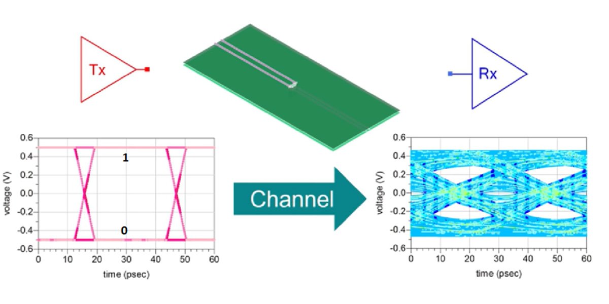
Maintaining good signal integrity is crucial for reducing EMI. High-speed signals should be routed carefully to minimize signal reflections, crosstalk, and ringing. Techniques such as controlled impedance routing, differential signaling, and proper termination can help improve signal integrity and reduce EMI.

3. PCB Layout
The PCB layout plays a significant role in managing EMI and EMC. Here are some layout considerations:
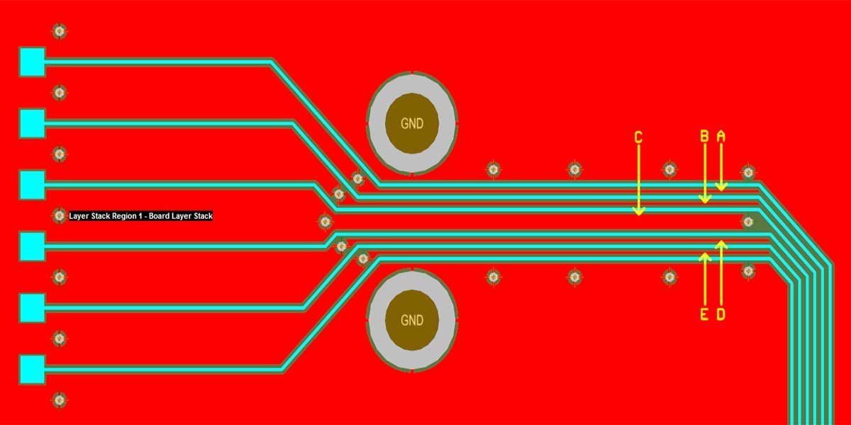
- a. Component Placement: Carefully consider the placement of components on the PCB to minimize the length of traces, loop areas, and coupling between sensitive components and noisy components.
- b. Trace Routing: Route traces to minimize their length and reduce loop areas. Keep high-speed signal traces away from sensitive analog or low-speed digital traces. Use differential routing for high-speed signals to improve noise immunity.
- c. Power and Ground Planes: Use dedicated power and ground planes to provide a low impedance return path for signals and reduce EMI. Ensure proper decoupling capacitors are placed near power pins of ICs to minimize power supply noise.
- d. EMI Filters: Incorporate EMI filters on input/output lines to suppress conducted emissions and protect against external noise sources.

4. Component Selection
Choose components that are designed for low EMI/EMC emissions and susceptibility. Look for components that meet relevant EMI/EMC standards and have appropriate shielding or filtering features.

5. Compliance Testing
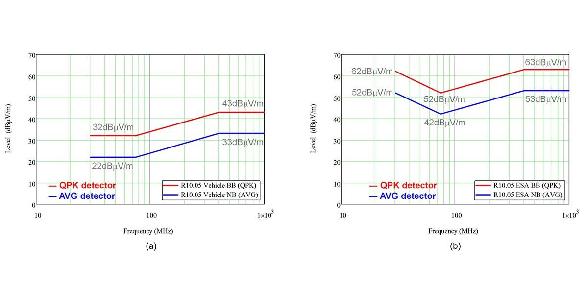
Once the PCB design is complete, it is essential to perform EMI/EMC compliance testing to ensure that the design meets the required standards. Compliance testing typically involves radiated and conducted emissions testing as well as susceptibility testing.
some additional details on EMI and EMC in PCB design:
6. EMI Sources
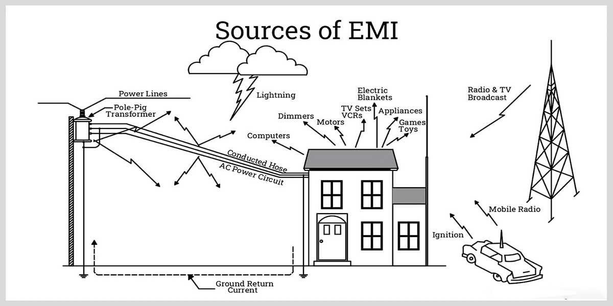
EMI can originate from various sources, both internal and external to the PCB. Internal sources include switching power supplies, high-speed digital circuits, and fast edge-rate signals. External sources can include nearby electronic devices, radio frequency (RF) transmitters, power lines, and electromagnetic radiation from the environment.

7. EMI Emission
EMI emission refers to the unwanted electromagnetic energy radiated by a PCB or conducted through its power and signal traces. This emission can interfere with the proper operation of other nearby electronic devices or disrupt sensitive circuitry on the same PCB.

8. EMI Susceptibility
EMI susceptibility, also known as EMI immunity, is the vulnerability of a PCB to external electromagnetic disturbances. It refers to the ability of the PCB to operate properly in the presence of electromagnetic interference without being adversely affected.
9. EMI Standards and Regulations
Various regulatory agencies, such as the Federal Communications Commission (FCC) in the United States and the International Electrotechnical Commission (IEC) globally, have set standards and regulations to limit EMI emissions from electronic devices. Compliance with these standards is necessary for commercial products to ensure electromagnetic compatibility and avoid interference with other devices.

10. Grounding
Proper grounding is crucial for managing EMI. Grounding provides a reference potential for the circuitry and helps minimize ground loops, which can induce unwanted noise. A solid ground plane or multiple ground planes can be used to provide low impedance paths for return currents and reduce EMI.

11. Signal Integrity
Maintaining good signal integrity helps minimize EMI. High-speed signals should be managed carefully to avoid signal degradation, ringing, and crosstalk, which can lead to increased emissions and susceptibility. Techniques such as controlled impedance routing, length matching, and careful placement of decoupling capacitors can improve signal integrity.
12. Crosstalk
Crosstalk occurs when signals on adjacent traces interfere with each other. It can lead to signal degradation and increased EMI. Techniques such as increasing spacing between traces, using differential signaling, and employing proper termination techniques can help mitigate crosstalk.

13. Filtering
EMI filters can be used to suppress conducted emissions and protect sensitive components from external noise sources. Common types of filters include ferrite beads, capacitors, and inductors. These components are placed in series or parallel with the power or signal lines to attenuate unwanted noise.

14. Simulation and Modeling
Advanced EMI simulation and modeling tools can be used to analyze and predict the behavior of PCB designs regarding EMI and EMC. These tools allow designers to identify potential sources of EMI, assess the effectiveness of mitigation techniques, and optimize the PCB layout for improved EMI performance.
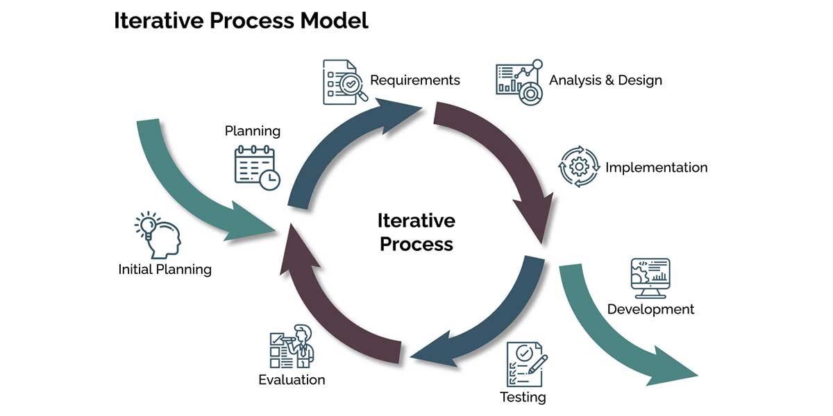
15. Design Iteration and Testing
EMI and EMC design is often an iterative process. Prototypes should be built and tested to verify compliance with relevant standards and regulations. Testing may involve radiated and conducted emissions measurements, susceptibility testing, and near-field and far-field scanning.
By carefully considering these aspects and employing appropriate design techniques, PCB designers can minimize EMI emissions, enhance EMC performance, and ensure the reliability and compatibility of their electronic products.