Printed Circuit Boards (PCBs) are crucial components in the electronics industry. Designing and manufacturing these boards require high precision and accuracy since even the smallest error can impact the overall performance of the circuit. One of the key tools in PCB production is the stencil, which is used for the precise application of materials onto the board. In this article, we will explore the role of stencils in the PCB production process, types of stencils, and their manufacturing and application methods.
What is a Stencil?
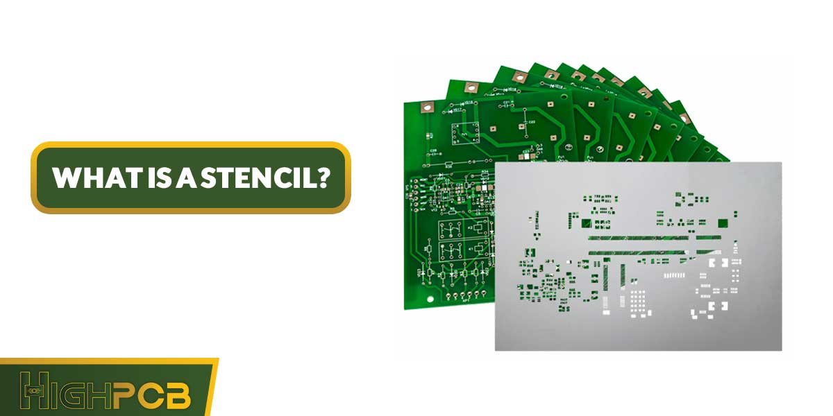
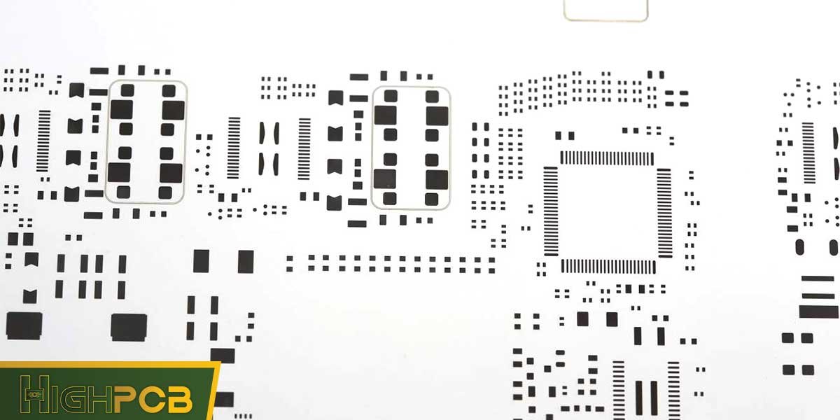
A stencil in PCB manufacturing is a thin sheet made of stainless steel or specific polymers, with holes that correspond to the circuit pattern. These holes define the points where solder paste or other materials are to be applied on the board.
Stencil Application in PCB Manufacturing
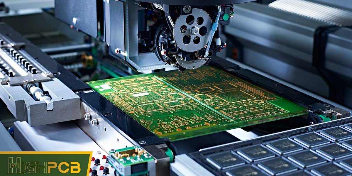
One critical step in PCB manufacturing is the application of solder paste on the exact points where electronic components will be placed. The stencil acts as a guide that allows the solder paste to be applied only on the desired locations. This high level of precision ensures that electronic components are correctly placed and soldered onto the board.
Types of Stencils
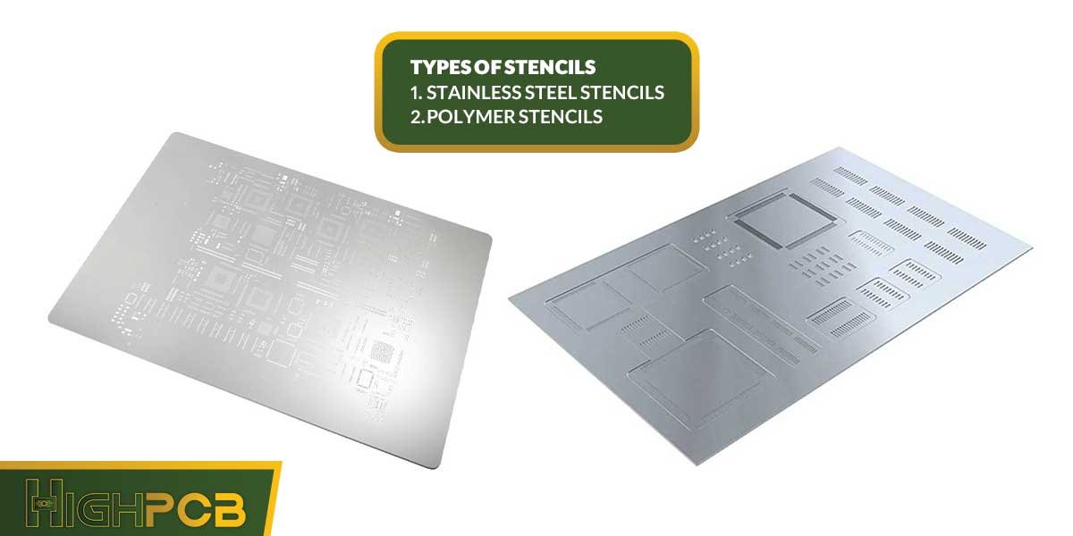
Stencils are categorized based on their material and structure:
- Stainless Steel Stencils: These are the most commonly used stencils in PCB production due to their high precision and resistance to wear. The holes in these stencils are created using lasers, which allows for excellent control and accuracy.
- Polymer Stencils: These stencils are used for specialized applications or low-volume production. Their flexibility and lower production cost are some of their key features.
Stencil Manufacturing Process
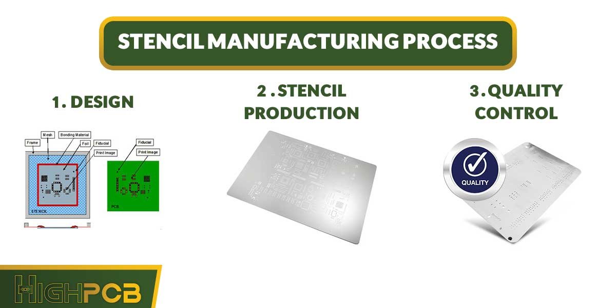
Manufacturing stencils is a precise and delicate process involving the following steps:
- Design: First, the PCB design and the points where the solder paste needs to be applied are created using specialized software.
- Stencil Production: After the design is approved, the stencil is created using laser devices or chemical methods. In the laser method, precise cuts are made on stainless steel sheets.
- Quality Control: Once produced, the stencils undergo thorough inspections to ensure the holes are accurately created without any deviations.
Advantages and Importance of Using Stencils in PCB Manufacturing
Using stencils in the PCB production process offers several advantages:
- High Precision: Stencils are designed and manufactured with laser technology, enabling precise material application.
- Reduced Production Errors: Stencils minimize human errors and enhance the final product’s quality.
- Increased Speed: In mass production, stencils optimize the process and reduce the time needed for applying solder paste.
Stencils are a key tool in PCB manufacturing that optimize the production process with high precision and quality, preventing potential errors. Given their importance in the electronics industry, using high-quality and accurate stencils is essential.
Multi-Level Stencils: A Solution for Advanced PCB Production
In the complex world of PCB manufacturing, various technologies and tools are used to enhance the precision and quality of the production process. One of these advanced tools is multi-level stencils. These stencils, known for their complex structure and multiple layers, enable precise material application, such as solder paste, in different areas of the PCB. In this article, we will discuss the advantages, challenges, production process, and crucial role of multi-level stencils in the electronics industry.
Introduction to Multi-Level Stencils
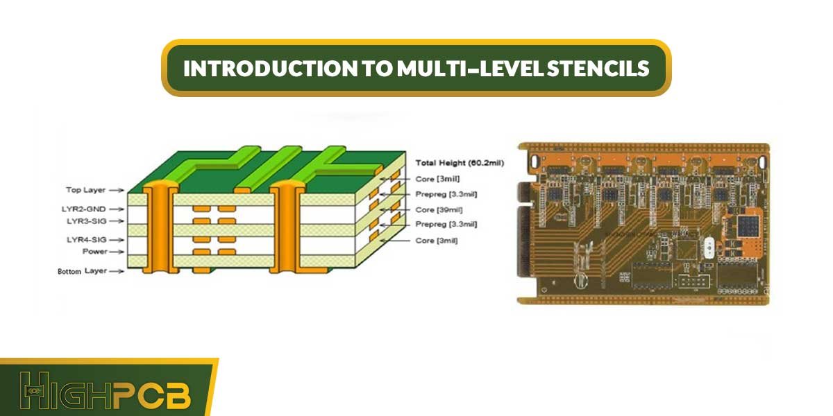
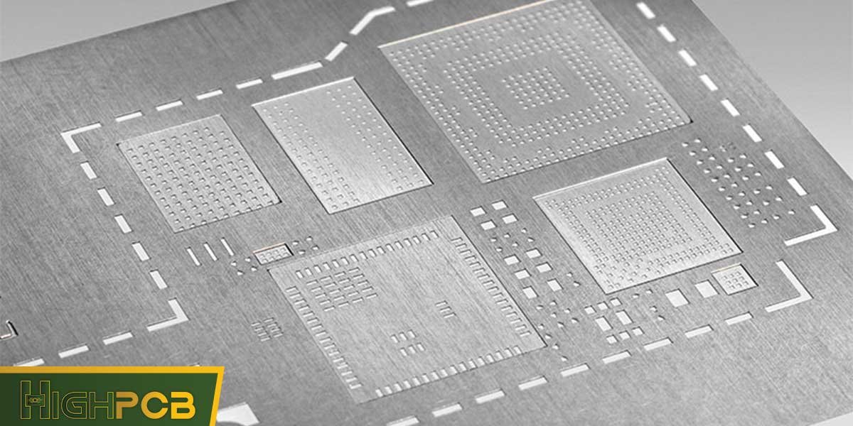
Multi-level stencils are stencils that utilize multiple layers with different thicknesses and patterns in their design and construction. These stencils are designed to control the exact thickness of materials in various areas of a PCB and are used for manufacturing complex and advanced boards, such as high-density interconnect (HDI) boards. Unlike single-layer stencils, which have a uniform thickness, multi-level stencils allow for adjusting the thickness in different parts of the board, making them the preferred choice for advanced projects.
In PCBs where the component sizes vary across the board, multi-level stencils are useful because the amount of solder paste applied on the pads needs to change accordingly. This adjustment is not possible with single-layer stencils.
Multi-Level Stencil Manufacturing Process
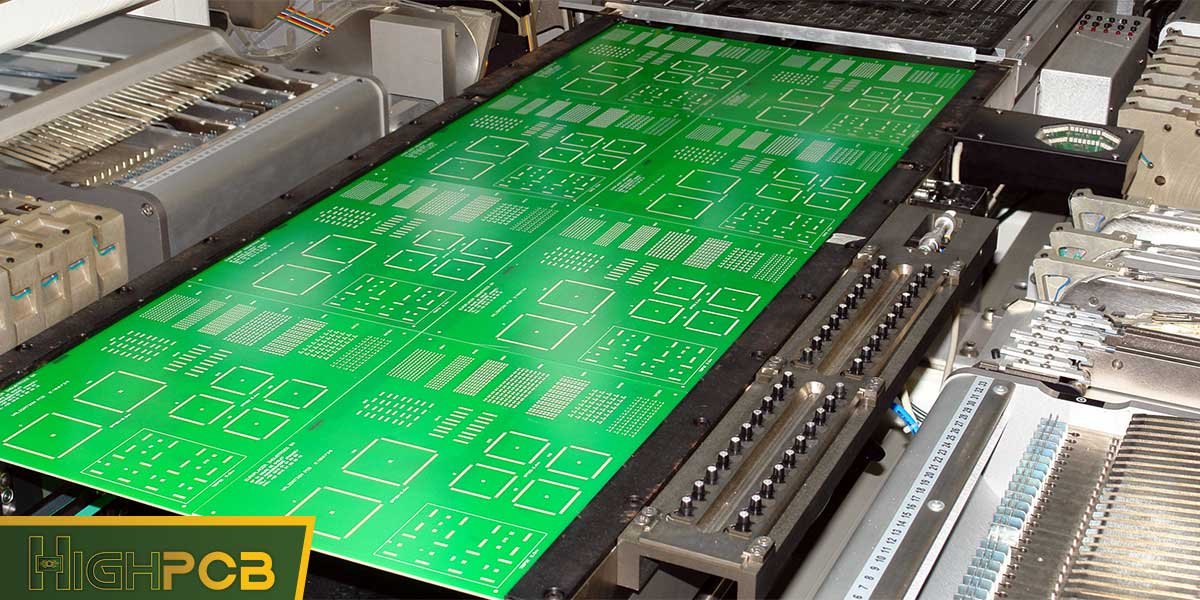
The production of multi-level stencils is a multi-step process that requires advanced equipment and specialized knowledge. The process is detailed below:
- Requirements Analysis and CAD Design:
The production of multi-level stencils begins with a detailed analysis of the project’s requirements. Engineers determine the necessary solder paste thickness and pattern for each section of the board. The design is then carried out in CAD software, where the different layer patterns, hole positions, and required thicknesses are defined. - Selection of High-Quality Materials:
Materials used in the production of multi-level stencils are typically high-grade stainless steel. These materials are selected for their durability, high precision, and resistance to corrosion. The thickness of the layers usually ranges from 100 to 300 microns, with thicker layers applied in specific areas as needed. - Layering and Pattern Creation Using Lithography:
In this stage, precise patterns are created on different stencil layers. Photolithography technology is used to create these patterns. The lithography process involves applying a photoresist layer onto the material, which is then exposed to light to form the desired patterns. These patterns determine where cuts should be made and how the varying thicknesses will be distributed. - Laser Cutting and Precision Machining:
After creating the patterns, laser cutting is used to precisely cut the holes and slots required in each layer. The cutting precision must be such that no defects or deviations occur in the final patterns. Due to its high accuracy and ability to produce micro-sized holes, laser cutting plays a critical role. Machining is also used in some areas for minor adjustments and pattern optimization. - Layer Assembly and Alignment:
Once the layers are cut and prepared, they are assembled to form the multi-level stencil. During this stage, the layers are stacked and aligned with high precision. Special mechanical techniques and adhesives are used to ensure accurate assembly without deviations. - Stencil Testing and Calibration:
After assembly, the produced stencil undergoes rigorous testing and calibration. This stage includes verifying the alignment of the patterns with the original CAD design and checking the uniformity of thickness and cutting accuracy. Quality control may involve using microscopes and optical tools to examine the details of the cuts and edges. - Final Cleaning and Packaging:
After completing the production and testing processes, the stencils are cleaned to remove any residual particles or potential contaminants. This cleaning is critical to prevent any interference during solder paste printing. The stencils are then packaged and prepared for delivery to PCB production lines. 
Applications of Multi-Level Stencils in the Electronics Industry
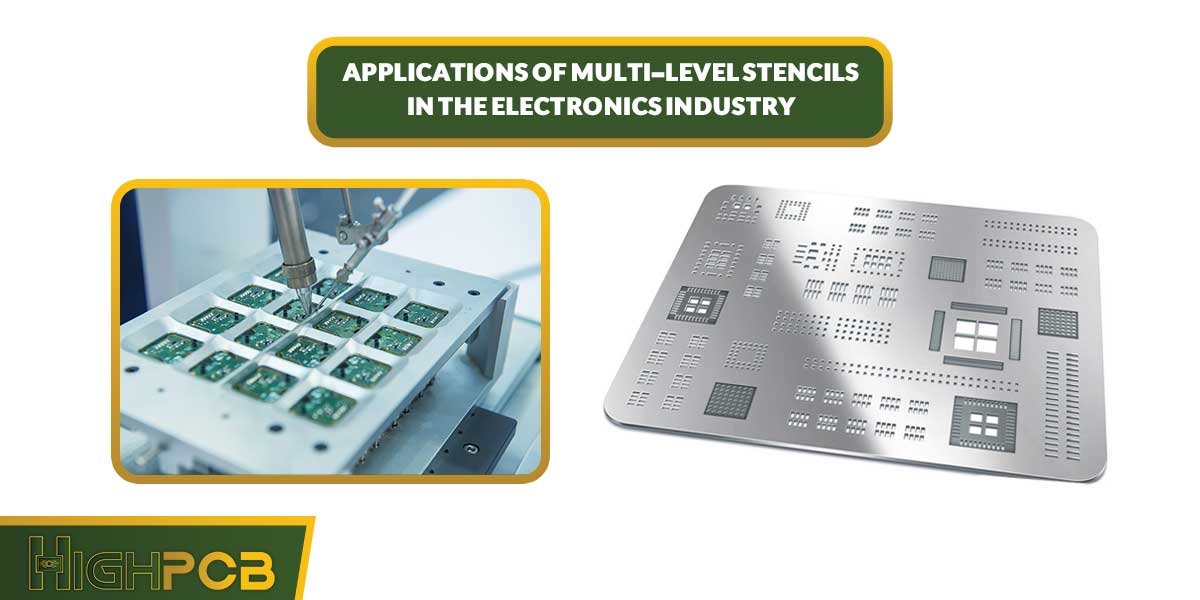
Multi-level stencils are widely used in situations requiring precise thickness control and printing in various board locations. Some of the main applications of these stencils include:
- High-Density Interconnect (HDI) PCBs:
HDI PCBs, where space is highly limited and many small components need to be placed, benefit from multi-level stencils. These stencils allow precise solder paste application with varying thicknesses, leading to higher quality and reduced assembly errors. - Micro and SMD Component Assembly:
In producing boards with very small components like microchips and surface-mount devices (SMDs), multi-level stencils play a crucial role. These components require accurate solder paste distribution, achievable only through multi-level stencils. - Manufacturing Sensitive and Advanced Equipment:
Industries such as medical, telecommunications, and aerospace, which require high precision and quality in electronic board production, extensively use multi-level stencils. These stencils reduce errors and ensure high-quality soldering, enhancing product quality and durability.
Advantages and Challenges of Using Multi-Level Stencils
Multi-level stencils offer several benefits to PCB manufacturers:
- Precise Control of Solder Paste Thickness: The ability to adjust solder paste thickness in different areas of the board improves soldering accuracy and reduces assembly issues.
- Increased Accuracy and Quality in Assembly Processes: Multi-level stencils enable more precise printing and reduce error rates, especially in complex boards with sensitive components.
- Improved Final Product Quality: The likelihood of issues such as improper connections or uneven soldering is reduced, leading to better product performance and reliability.
- Lower Rework and Repair Costs: The high accuracy of multi-level stencils significantly reduces the need for rework and repairs, leading to cost savings.
However, using multi-level stencils also presents specific challenges:
- High Production Costs: The complex process and advanced equipment required for multi-level stencils make them expensive to produce, which can impact projects involving large-scale production.
- Need for Advanced Technical Knowledge: Designing and manufacturing multi-level stencils requires substantial technical expertise and experience. Mistakes in design or production can cause significant problems in PCB manufacturing.
- More Challenging Maintenance and Cleaning: Due to their complex structure and multiple layers, multi-level stencils require careful maintenance and cleaning to prevent clogging and maintain printing accuracy.
Recent Advances in Multi-Level Stencils
With advancements in technology and the increasing demand for highly accurate and complex PCBs, multi-level stencil technology is rapidly evolving. Some recent innovations in this area include:
- Use of Advanced Materials: Specialized alloys and corrosion-resistant coatings are being used to extend stencil lifespan and reduce wear over time.
- Improved Lithography Techniques: Advanced optical lithography techniques, including ultraviolet lithography, are being employed to create more precise patterns and reduce hole sizes to the nanometer scale.
- Automation and Smart Manufacturing: Intelligent systems and robotics are increasingly being used in the design, production, and testing processes to enhance accuracy and reduce errors.
Conclusion
Multi-level stencils are a strategic tool in the production of high-precision and high-quality PCBs, playing a crucial role in the electronics industry. As the demand for more complex boards with higher component density continues to grow, these stencils have become a key component in the production process. Although the production of multi-level stencils involves high costs and challenges, the significant improvements in final product quality, precision, and reduced repair costs make them an invaluable asset for PCB manufacturers.


