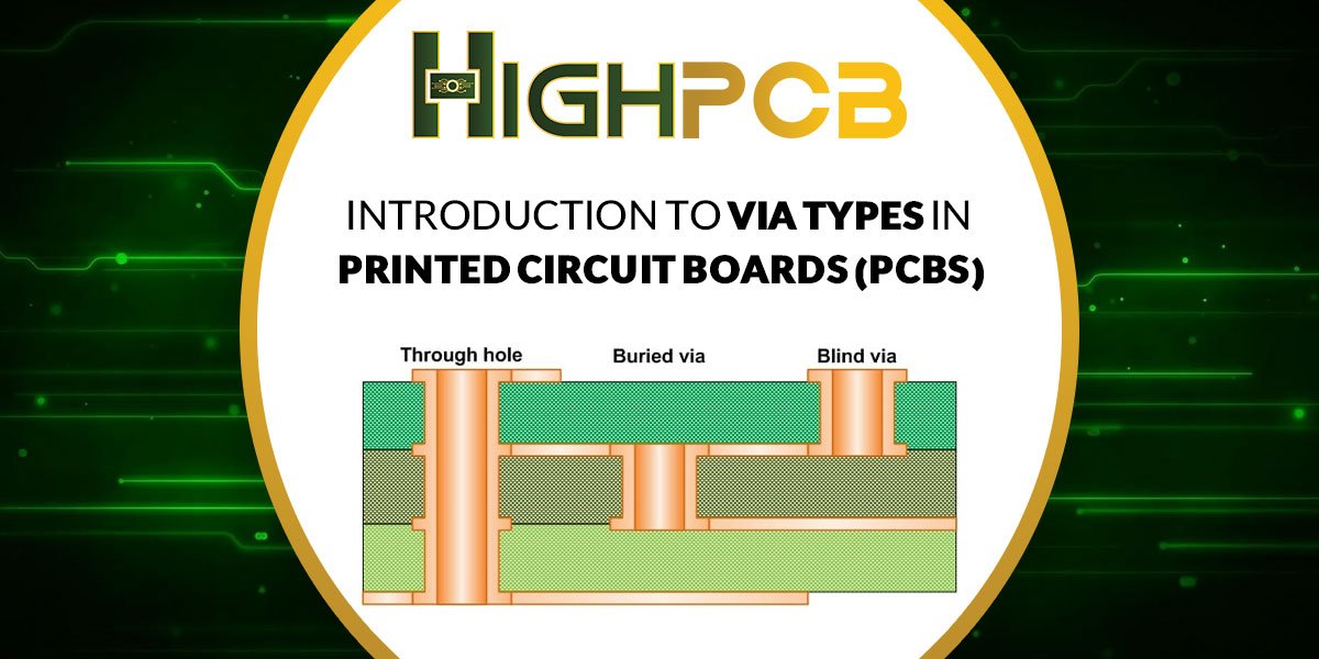
Printed Circuit Boards (PCBs) are indispensable components in modern electronic devices, serving as the foundation upon which electronic circuits are built. A crucial element in PCB design is the use of vias, small holes that facilitate electrical connections between the different layers of a PCB. These vias play a significant role in the performance, reliability, and compactness of electronic devices. This article delves into the various types of vias used in PCBs, their unique characteristics, and their specific applications, providing a comprehensive understanding for anyone involved in electronics design and manufacturing.
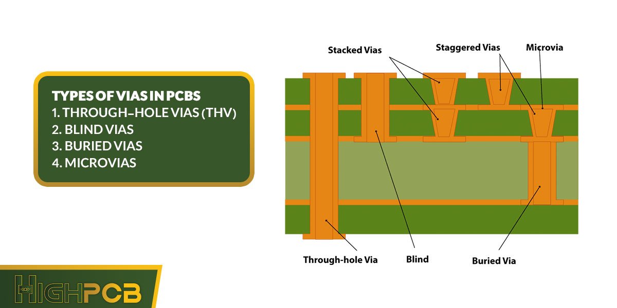
Types of Vias in PCBs
- Through-Hole Vias (THV)
- Blind Vias
- Buried Vias
- Microvias
1. Through-Hole Vias (THV)
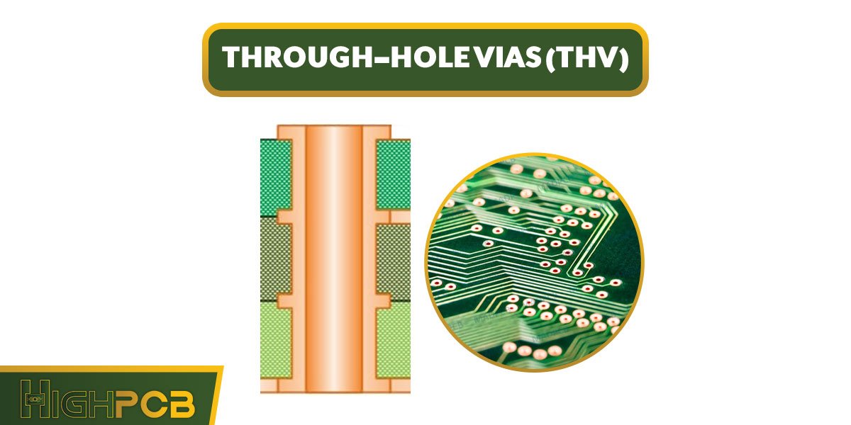
Through-Hole Vias are the most traditional and widely used type of vias in PCB manufacturing. They extend through the entire thickness of the PCB, connecting all the layers from the top to the bottom. These vias are typically drilled mechanically and then plated with copper to ensure electrical connectivity.
Key Characteristics
- Large Diameter: Through-hole vias have a larger diameter compared to other via types, typically ranging from 0.15 mm to 0.3 mm.
- High Reliability: Due to their robust construction, through-hole vias offer high mechanical strength and reliability.
Applications
- High Current Carrying Capacity: The larger size of through-hole vias allows them to handle higher current loads, making them ideal for power and ground connections in PCBs.
- Mechanical Strength: Through-hole vias provide strong mechanical support, which is essential for mounting heavy components such as connectors, large capacitors, and transformers.
- Double-Sided and Multi-Layer Boards: These vias are commonly used in both double-sided and multi-layer boards, providing reliable connections across all layers.
Through-hole vias are essential in applications where mechanical strength and high current capacity are critical, such as in power supplies, automotive electronics, and industrial equipment.
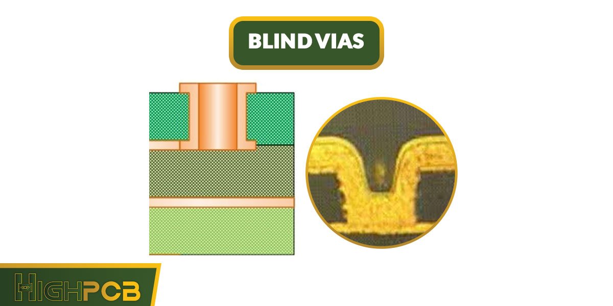
Blind Vias
Blind Vias are used to connect the outer layer of the PCB to one or more inner layers without passing through the entire board. These vias are typically used in multi-layer PCBs to optimize space and improve electrical performance.
Key Characteristics
- Partial Depth: Blind vias are drilled only to a specific depth, connecting the surface layer to one or more internal layers.
- Smaller Diameter: They generally have a smaller diameter than through-hole vias, which helps in conserving PCB real estate.
Applications
- High-Density Interconnect (HDI) Boards: Blind vias are crucial in HDI PCBs, where space is at a premium and component density is high. They allow for more efficient routing of traces and connections without compromising on space.
- Signal Integrity: By minimizing the length of the connections between layers, blind vias help reduce signal loss and electromagnetic interference, which is vital in high-speed and high-frequency circuits.
- Compact Designs: Blind vias are used in compact electronic devices such as smartphones, tablets, and wearable technology, where minimizing the size of the PCB is essential.
Blind vias are particularly beneficial in applications requiring high component density and high-speed signal transmission, such as telecommunications equipment, consumer electronics, and medical devices.
Buried Vias
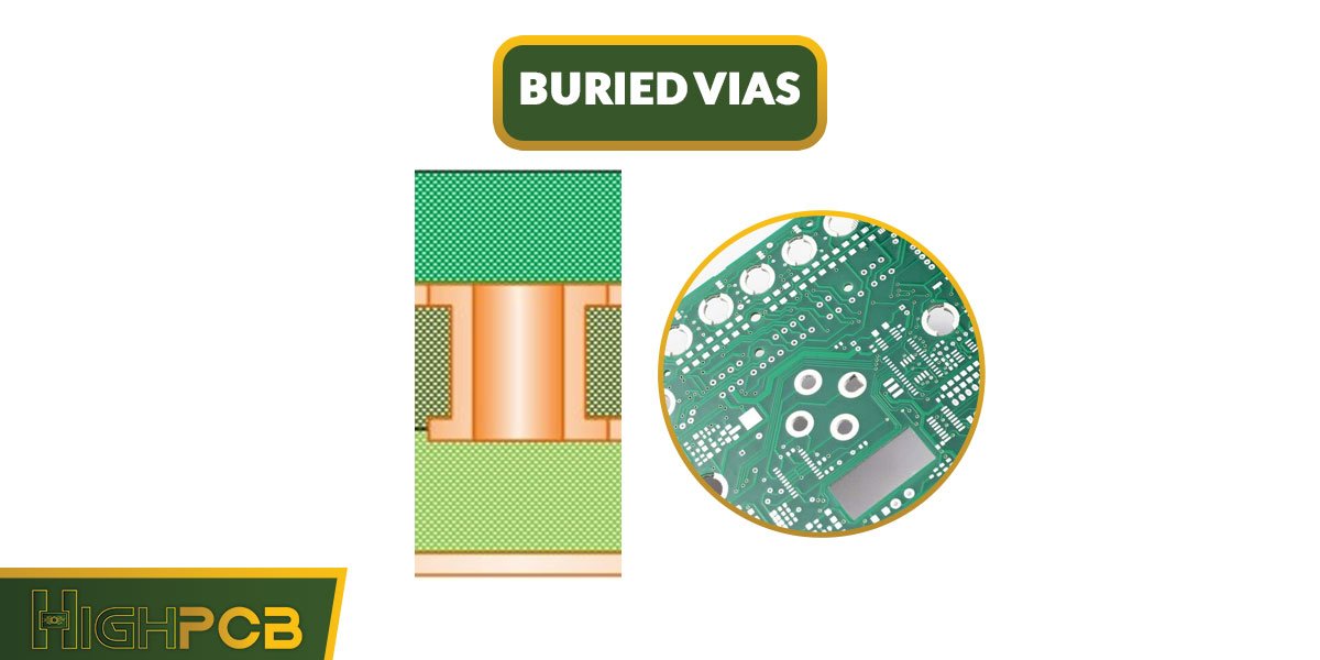
Buried Vias are entirely encapsulated within the PCB, connecting one or more inner layers without reaching the outer layers. These vias are drilled and plated before the PCB layers are laminated together.
Key Characteristics
- Invisible from the Surface: Buried vias do not appear on the surface layers of the PCB, allowing for more complex internal connections.
- Space Efficient: By keeping the connections internal, buried vias free up space on the surface layers for other components and traces.
Applications
- Complex Multi-Layer Boards: Buried vias enable designers to create more complex multi-layer PCBs with intricate routing between internal layers without affecting the surface layout.
- High-Density Applications: In high-density PCBs, buried vias allow for efficient use of space, enabling more connections and components in a smaller area.
- Signal Routing: Buried vias are used in situations where internal layer connections are necessary for signal routing, power distribution, and ground planes without interfering with surface-mounted components.
Buried vias are ideal for applications requiring complex internal layer connections, such as advanced computing systems, aerospace electronics, and sophisticated industrial controls.
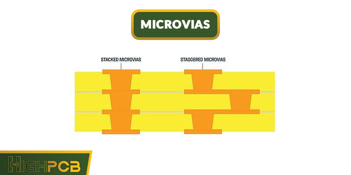
Microvias
Microvias are small-diameter vias typically created using laser drilling techniques. They are used in HDI PCBs to connect adjacent layers and can be categorized into different types based on their layout and stacking.
Key Characteristics
- Very Small Diameter: Microvias usually have a diameter of less than 0.15 mm, significantly smaller than traditional vias.
- Laser Drilled: The precision of laser drilling allows for extremely accurate and consistent microvia formation.
Applications
- Advanced HDI Designs: Microvias are essential in advanced HDI PCBs, enabling extremely high component densities and complex routing solutions. They are widely used in cutting-edge consumer electronics like smartphones, tablets, and wearable devices.
- Improved Signal Integrity: Due to their small size, microvias reduce parasitic inductance and capacitance, improving signal integrity and performance in high-speed and high-frequency applications.
- Layer-to-Layer Connections: Microvias are often used for layer-to-layer connections in multi-layer PCBs, allowing for efficient vertical interconnections with minimal space requirements.
Microvias are indispensable in the design of high-performance electronic devices, providing the necessary connections in compact, high-density configurations.
Selecting the Right Via Type
The choice of via type in PCB design depends on several factors, including board complexity, electrical requirements, and space constraints. Here are some considerations for selecting the appropriate via type:
- Board Complexity: For simple double-sided boards, through-hole vias may suffice. However, for multi-layer and HDI boards, a combination of blind, buried, and microvias may be necessary to achieve the desired connectivity and performance.
- Electrical Requirements: High-current applications benefit from the robustness of through-hole vias, while high-speed and high-frequency circuits require vias that minimize signal loss, such as blind vias and microvias.
- Space Constraints: In compact electronic devices, blind and buried vias help optimize space without compromising functionality. Microvias are particularly useful in miniaturized designs where every millimeter of space counts.
Conclusion
Understanding the different via types in PCBs and their applications is essential for designing efficient and reliable electronic devices. Each via type offers unique advantages and is suited to specific applications, from robust through-hole vias to space-saving blind and buried vias, and high-performance microvias. By selecting the right via type, engineers can optimize PCB design to meet the demands of modern electronics, ensuring performance, reliability, and miniaturization.
Whether you are designing a simple two-layer board or a complex multi-layer HDI PCB, incorporating the appropriate vias will significantly impact the overall functionality and success of your project. By leveraging the strengths of each via type, you can create PCBs that are not only compact and efficient but also capable of supporting the advanced features and high performance required by today’s electronic devices.


