In the field of printed circuit board (PCB) manufacturing, quality control and precise analysis are essential for ensuring reliability and performance. One critical process that helps achieve these goals is microsectioning. For PCB manufacturers like HighPCB, microsectioning plays a crucial role in verifying the integrity of PCBs, identifying potential defects, and maintaining high standards of production.
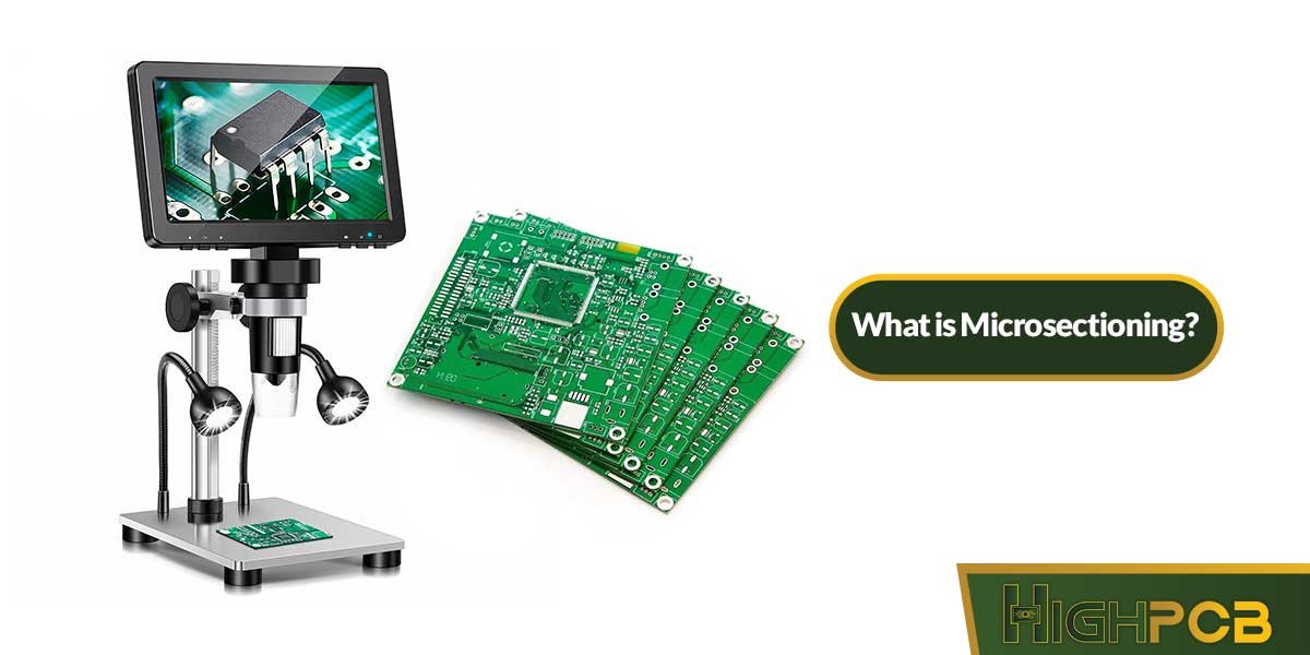
What is Microsectioning?
Microsectioning, also known as cross-sectioning, is a technique used to examine the internal structure of PCBs by slicing through the board to reveal specific layers and features. This procedure allows manufacturers to evaluate the quality of vias (vertical interconnect accesses), plating thickness, material composition, and other critical aspects that may not be visible from the surface.
At its core, microsectioning involves cutting a sample of the PCB, embedding it in a resin for stability, grinding, and polishing it to a mirror-like finish. The final step involves examining the prepared sample under a microscope to inspect features such as layer bonding, voids, and defects.
Why is Microsectioning Important in PCB Manufacturing?
Microsectioning provides an unparalleled view of the internal structure of PCBs, offering manufacturers the ability to perform detailed failure analysis and quality control. It is used throughout the production process to inspect finished products or diagnose issues that arise during manufacturing.
Here are some of the key reasons why microsectioning is indispensable in PCB production:
- Defect Identification: One of the primary uses of microsectioning is identifying defects in the internal structure of PCBs. These defects could range from poor layer bonding to insufficient copper plating or even voids in solder joints. Without this process, it would be nearly impossible to detect such issues before the product reaches the client, which could result in failures in the field.
- Quality Control: Manufacturers like HighPCB use microsectioning to ensure their products meet strict industry standards. The technique helps verify whether the internal features of the PCB comply with the required specifications, including material thickness, plating, and via structures. This is especially critical when producing PCBs for high-reliability applications such as medical devices or aerospace systems.
- Failure Analysis: When a PCB fails during operation, microsectioning can be used to determine the root cause. This helps manufacturers identify process errors, material defects, or design flaws that may have led to the failure. In many cases, this detailed analysis can prevent future failures by guiding design improvements or adjustments in the production process.
- Precision and Accuracy: Unlike other inspection methods, microsectioning provides a microscopic view of the PCB, revealing fine details about layer adhesion, drilling quality, and via plating. This level of precision is necessary for high-end PCBs, where even a minor defect can lead to significant performance issues.
The Process of Microsectioning: Step-by-Step
Understanding the microsectioning process is key to appreciating its value. Below is a step-by-step overview of how it works in a PCB manufacturing environment:
- Sample Selection: The first step involves selecting a sample area on the PCB that needs to be examined. This could be a critical via, a specific trace, or an area where defects are suspected.
- Mounting the Sample: The selected sample is then mounted in a specialized resin, which stabilizes the board and makes it easier to handle during the grinding and polishing steps.
- Cutting: Using precise cutting tools, a small section of the PCB is sliced. The objective here is to expose the exact layers or features that need inspection without damaging the rest of the board.
- Grinding and Polishing: After the sample is cut, it undergoes a series of grinding and polishing steps to achieve a smooth, mirror-like finish. This ensures that all features can be clearly observed under a microscope.
- Microscopic Examination: The final step is examining the prepared sample under a high-power microscope. During this phase, engineers analyze the quality of the plating, bonding between layers, and any defects like voids or cracks.
Advantages of Using Microsectioning for PCB Analysis
Microsectioning offers numerous advantages, making it a preferred technique for PCB manufacturers who prioritize quality and reliability. Let’s explore the key benefits:
- In-depth Internal Inspection: Unlike surface inspection techniques such as visual checks or X-ray imaging, microsectioning allows manufacturers to look deep into the board. This enables the detection of issues such as layer misalignment, voids, and material inconsistencies.
- Improved Reliability: By identifying potential problems early in the manufacturing process, microsectioning helps manufacturers prevent faulty products from reaching customers. This enhances the overall reliability of the product, reducing the likelihood of failures in the field.
- Enhanced Product Life Cycle: PCBs that undergo thorough internal inspection through microsectioning tend to have a longer lifespan. Detecting and addressing issues such as poor plating or weak solder joints ensures that the final product is robust and can withstand the rigors of its intended application.
- Cost Savings: Early detection of defects can save significant costs in the long run. By catching problems during the manufacturing process, companies like HighPCB can avoid costly product recalls, warranty claims, and customer dissatisfaction. Additionally, it helps minimize waste by allowing manufacturers to adjust their processes as needed.
- Compliance with Industry Standards: For many industries, including automotive, aerospace, and medical sectors, strict regulatory standards must be met. Microsectioning helps ensure that PCBs comply with these regulations, allowing manufacturers to demonstrate the quality and reliability of their products.
- Tailored Solutions: Microsectioning also enables manufacturers to customize their solutions. By closely analyzing the specific needs of a project, companies like HighPCB can adjust the manufacturing process to meet the unique requirements of their clients. Whether it’s increasing the thickness of a copper layer or improving via strength, microsectioning provides the insights needed for tailored adjustments.

HighPCB’s Expertise in Microsectioning
At HighPCB, we understand that quality is non-negotiable. Our extensive experience in microsectioning ensures that every PCB we produce meets the highest standards. We utilize advanced tools and state-of-the-art techniques to provide our clients with detailed insights into the internal structure of their boards.
Our commitment to delivering top-notch products is evident in our rigorous testing and inspection processes. Microsectioning is just one of the many tools we use to ensure that every PCB leaving our facility is flawless, reliable, and ready for its intended application.
Conclusion
Microsectioning is an indispensable tool in modern PCB manufacturing, offering unparalleled insights into the internal structure of printed circuit boards. It allows manufacturers to detect defects, improve reliability, and ensure compliance with industry standards. For HighPCB, this process is a key component of our quality control strategy, helping us deliver products that meet the high expectations of our clients.
By integrating microsectioning into your manufacturing process, you can enhance product performance, reduce the risk of failure, and ultimately deliver superior products to your customers.