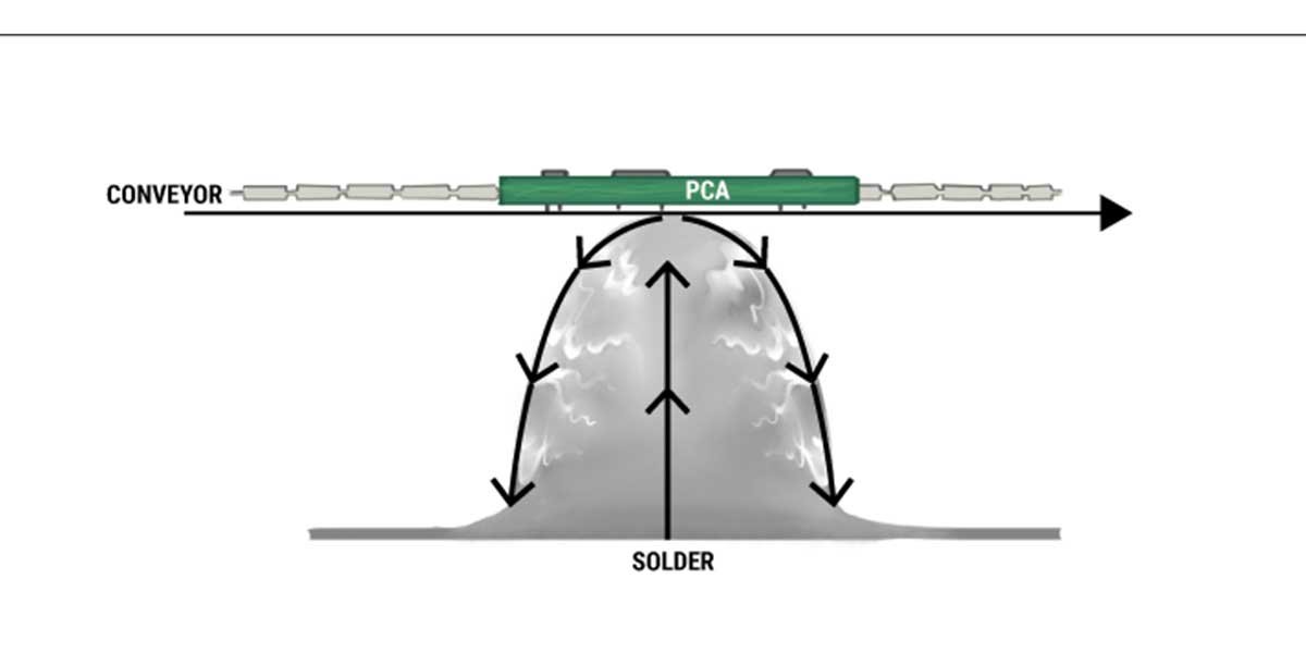
Wave soldering is a common method used for soldering electronic components onto printed circuit boards (PCBs) during the manufacturing process. It is primarily used for through-hole components, which have leads that pass through holes in the PCB.
The process of wave soldering involves the following steps:
- Preparation: Before wave soldering, the PCB is prepared by applying solder paste onto the surface mount pads where the components will be placed. This is done using a stencil or a screen printing process.
- Component placement: The components are then placed onto the PCB, aligning the component leads with the corresponding pads. This can be done manually or using automated pick-and-place machines.
- Preheating: The PCB is preheated to remove any moisture and to ensure that the components are at a suitable temperature for soldering. This is typically done in a preheating oven or a dedicated preheating station.
- Flux application: Flux is applied to the areas to be soldered. Flux is a chemical substance that helps clean the metal surfaces and promotes the soldering process by removing oxides and ensuring good wetting of the solder.
- Wave soldering: The PCB is then passed over a wave soldering machine. The machine has a pool of molten solder, usually a mixture of tin and lead, which is kept at a controlled temperature. A pump generates a wave of molten solder that flows over the exposed pads and component leads. The wave soldering machine is designed in such a way that it only contacts the bottom side of the PCB, leaving the components on the top side unaffected.
- Solder solidification: As the wave passes over the components, it melts the solder paste and forms a solder joint between the component leads and the PCB pads. The solder solidifies as the PCB moves away from the wave.
- Cleaning and inspection: After wave soldering, the PCB is usually cleaned to remove any flux residues or other contaminants. The board is then inspected for any soldering defects, such as insufficient solder, bridging between adjacent pads, or misaligned components.
Working on a PCB involves various tasks depending on the stage of the manufacturing process. Here are some common steps in PCB assembly:
- Component preparation: This involves gathering the necessary components, ensuring they are undamaged, and preparing them for placement. This may include cutting component leads to the appropriate length, taping or packaging components, or applying adhesive if required.
- Solder paste application: If surface mount technology (SMT) components are used, solder paste is typically applied to the PCB pads using a stencil or a screen printing process. This step requires precision to ensure the correct amount of solder paste is applied to each pad.
- Component placement: SMT components are typically placed on the PCB using automated pick-and-place machines. These machines can quickly and accurately position components on the PCB according to the design specifications. For through-hole components, manual placement is often necessary, aligning the component leads with the corresponding holes in the PCB.
- Reflow soldering: After component placement, the PCB is typically subjected to a reflow soldering process. The PCB is heated in a reflow oven, causing the solder paste to melt and form solder joints between the components and the PCB.
- Inspection and testing: Once the soldering process is complete, the PCB is inspected for any soldering defects, such as misaligned components, insufficient solder, or solder bridging. Automated optical inspection (AOI) and X-ray inspection are commonly used for this purpose. Additionally, functional testing may be performed to ensure the assembled PCB operates correctly.
It’s worth noting that working with PCBs requires knowledge of electronic components, soldering techniques, and familiarity with assembly processes. Proper training and experience are essential for ensuring reliable and high-quality PCB assemblies.