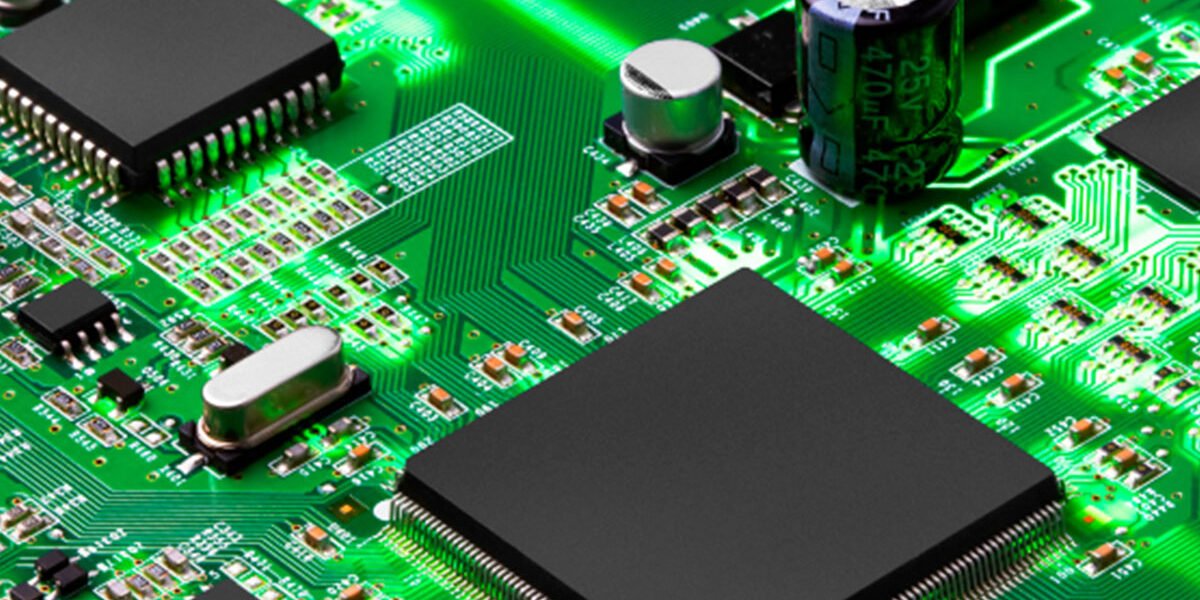
The word PCB is an abbreviation of Printed Circuit Board, which means printed circuit board. In the following article, we intend to explain everything about electronic boards to you in the simplest way.
What is PCB design?
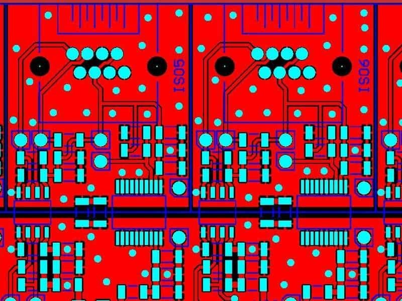
PCB design is also called electronic board design or printed circuit board design. After the schematic design, it is essential for creating electronic devices and tools; Various software is used to design the electronic board, one of the most famous of which is Altium Designer.
What are printed circuit boards or PCBs made of?
PCBs are made of different materials such as Teflon, Rogers, Flexi (flexible boards), and fiber, Each of these alone includes different subgroups; the most crucial characteristic of them is their dielectric coefficient, which is determined according to the type of circuit and its application in various industries such as automotive, commercial, military, industrial, etc.
What is a multilayer board?
Printed circuit boards are designed in the form of 1-layer, 2-layer, and multilayer boards.

- 1-layer boards:
Some boards only have lead-tin on one side, and the parts are assembled on only one side.
1-layer or one-sided copper boards are not metalized; even at the customer’s request, a solder mask may not be considered. - 2-layer boards:
The two-layer boards are copper-plated and metalized on both sides. The part is assembled on both sides of the two-layer boards (double-sided metallization). To prevent connections on the board, it is highly recommended to use protective printing (Solder Mask). - Multilayer boards:
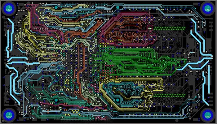
4-layer, 8-layer, 12-layer, 16-layer, and 32-layer boards are called multilayer boards used for complex and advanced designs.
There are other reasons for using multilayer boards, which can be mentioned to reduce the dimensions of the board, which ultimately causes the final product to shrink and reduce its weight.
Due to the progress of science and the shrinking of elements, we are forced to make a unique design by observing all the points and principles of design. The only way to implement a correct design is to use multilayer boards, which is fully discussed in the section on observing design principles.
The construction and production of these boards are done with the help of advanced tools and equipment, and not every country can make a series of these multilayer boards.
 Thickness
The thickness of electronic boards is designed from 0.2 to 3.2 according to their application and the number of layers.
Via
On 2-layer and multilayer boards, holes are created for connections between layers called Via. For example, if we want to transfer a line (crack or line) from under the board to the board in the design of the board (PCB), we put a via there, Then we continue the line on the board.
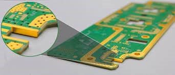
Metalized boards are plated inside their holes after drilling. Plating causes the inner wall of the holes to be covered with a thin copper layer to create a connection between the layers. Also, after electroplating, a layer of lead-tin is added to Via; in addition to copper, PCB can also be plated with gold.
The appropriate thickness of the plating layer is 25 microns of copper on the hole wall. “Every 1 micron is equal to 0.001 mm.
 Gerber file
The printed circuit board format designed in Altium software is PCBDOC; to separate the layers and increase the reliability factor, we take the output from Altium software and refer it to the board manufacturer.
Advantages of Gerber output:
- There is no need to send the source file, so the security of your work will be maintained.
- When you get Gerber with your software and send it for construction, you are sure that no changes will be made to your file during construction Because there may be unwanted changes in the file due to changing the software version.
- The size of your file will be significantly reduced, so you will have no problem sending it.
- When capturing, all values of elements and parts are removed, And you are sure that no one can easily copy your design.
HIGHPCB, with a professional team and a brilliant history in attracting customer trust, is ready to design, manufacture, and supply components and assemble the PCB you need.


 Thickness
 Gerber file


