")
Designing a Printed Circuit Board (PCB) requires precision, attention to detail, and a deep understanding of both the electrical and mechanical aspects of the circuit. As technology continues to evolve, designers must stay updated on best practices to ensure their PCBs meet modern performance and reliability standards.In this comprehensive guide, we will explore the most common PCB design mistakes to avoid in 2025 and provide insights on how to improve your design process.
1. Inadequate Planning and Requirements Analysis
One of the most critical mistakes in PCB design is starting without a clear understanding of the project requirements. Skipping this step can lead to costly redesigns and project delays.
Common Issues:
- Undefined electrical specifications.
- Unclear mechanical constraints.
- Lack of consideration for environmental factors (temperature, humidity, etc.).
How to Avoid:
- Conduct a thorough requirements analysis before starting the design.
- Collaborate with stakeholders to gather all necessary information.
- Use project management tools to document and track requirements.
Pro Tip: Use simulation tools like SPICE or LTspice to validate your circuit design before creating the PCB layout.
2. Poor Component Placement
Component placement is crucial for ensuring signal integrity, thermal management, and manufacturability.
Common Issues:
- Random placement of components.
- Placing high-speed components too far from each other.
- Ignoring thermal considerations.
How to Avoid:
- Group related components logically to minimize trace lengths.
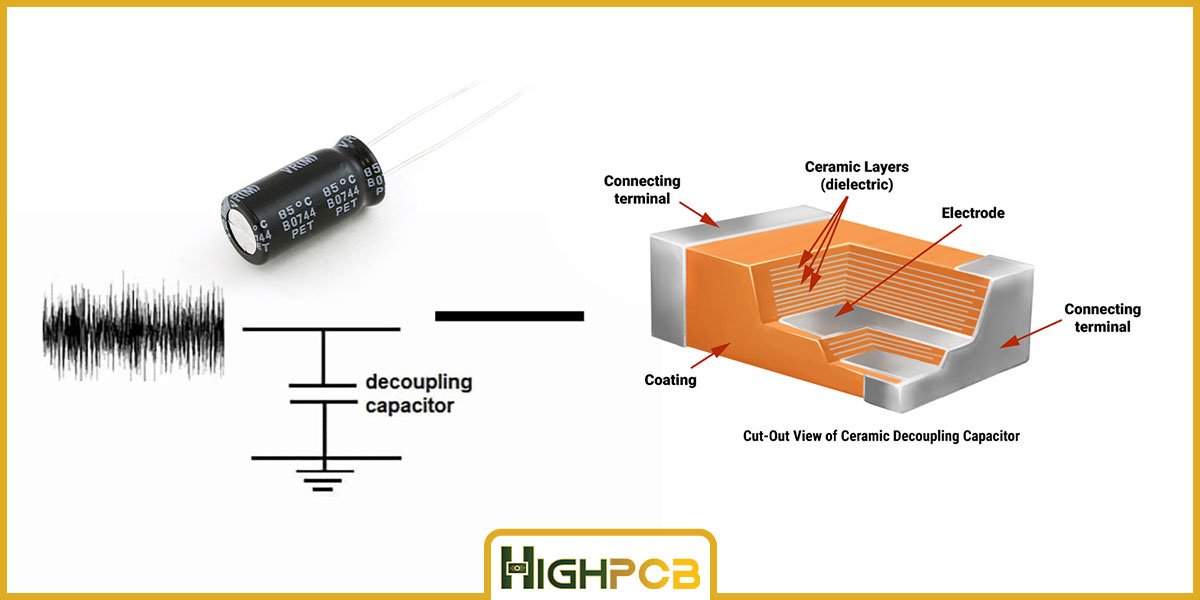
- Place decoupling capacitors as close as possible to power pins.
- Ensure proper spacing for thermal dissipation.
Pro Tip: Use CAD software with auto-placement features to optimize your layout.
3. Ignoring Signal Integrity
In high-speed designs, signal integrity is a critical factor that can significantly impact performance.
Common Issues:
- Inconsistent trace widths.
- Poor impedance matching.
- Inadequate ground planes.
How to Avoid:
- Maintain consistent trace widths for critical signals.
- Use impedance calculators to ensure proper matching.
- Implement continuous ground planes to reduce noise.
Pro Tip: For high-frequency designs, use materials with low dielectric constants to minimize signal loss.
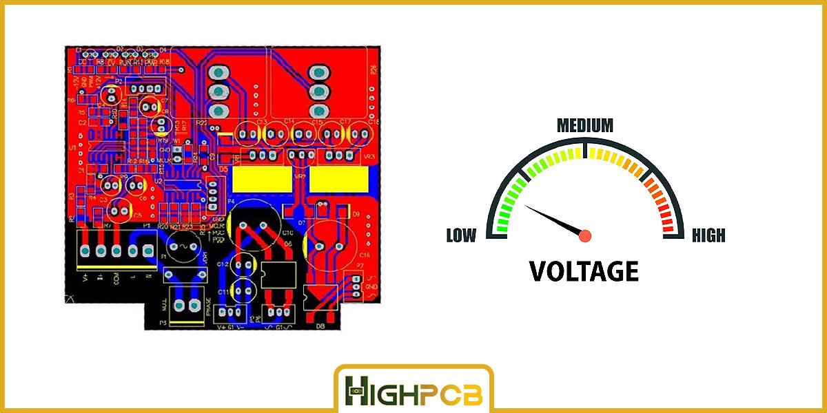
4. Inadequate Power Distribution Network (PDN)
A poorly designed PDN can cause voltage drops, noise, and unstable power delivery.
Common Issues:
- Thin power traces.
- Inadequate decoupling capacitors.
- Incorrect placement of vias.
How to Avoid:
- Use wide power traces and multiple ground planes.
- Place decoupling capacitors near power pins.
- Optimize via placement to reduce resistance.
Pro Tip: Use PDN analysis tools to identify and fix potential issues early in the design process.
5. Ignoring Design for Manufacturability (DFM)
Even a perfectly functioning PCB design can fail during manufacturing if it doesn’t adhere to DFM guidelines.
Common Issues:
- Using non-standard component footprints.
- Ignoring PCB manufacturer’s capabilities.
- Overcomplicating the design.
How to Avoid:
- Consult with your PCB manufacturer early in the design process.
- Follow industry standards like IPC-2221 for PCB design.
- Simplify your design where possible.
Pro Tip: Use a DFM checklist to ensure your design meets manufacturing requirements.
6. Inadequate Thermal Management
Overheating can cause PCB failure, especially in high-power applications.
Common Issues:
- Insufficient heat sinks.
- Poor placement of thermal vias.
- Ignoring airflow considerations.
How to Avoid:
- Use thermal vias to transfer heat away from hot spots.
- Implement heat sinks where necessary.
- Design for proper airflow within the enclosure.
Pro Tip: Use thermal simulation tools to predict and mitigate heat-related issues.
7. Overlooking EMC/EMI Considerations
Electromagnetic compatibility (EMC) and electromagnetic interference (EMI) can cause malfunctions in electronic devices.
Common Issues:
- Inadequate shielding.
- Poor grounding practices.
- Long trace lengths.
How to Avoid:
- Use proper shielding techniques.
- Minimize trace lengths for critical signals.
- Implement robust grounding strategies.
Pro Tip: Follow industry standards like IEC 61000-4-3 for EMC testing.
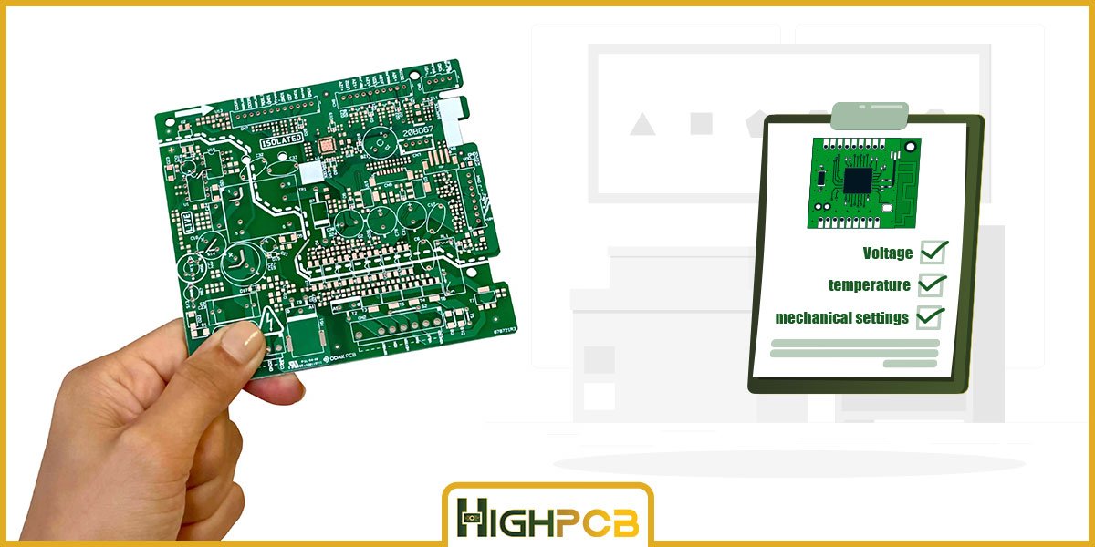
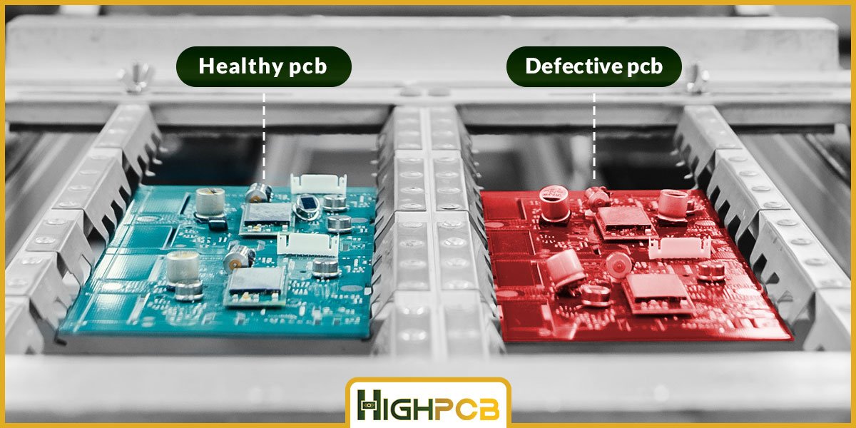
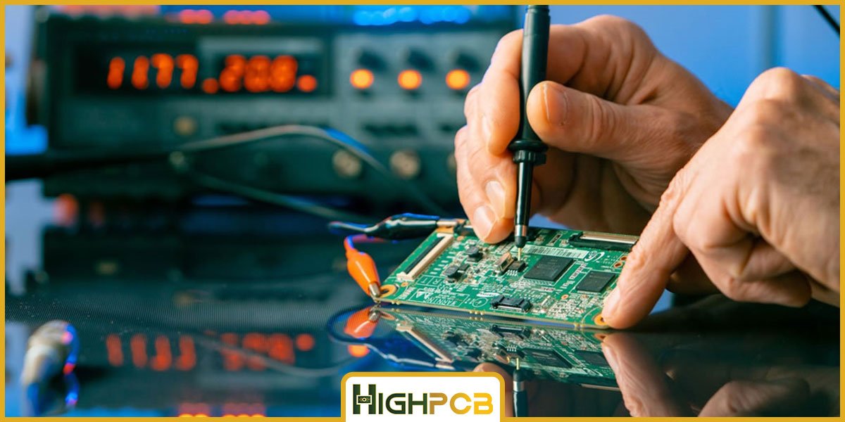
8. Failing to Test and Validate the Design
Skipping the testing phase can lead to costly failures in the field.
Common Issues:
- Skipping prototype testing.
- Inadequate functional testing.
- Ignoring environmental testing.
How to Avoid:
- Build prototypes for each design iteration.
- Perform functional and environmental tests.
- Use automated test equipment (ATE) for thorough validation.
Pro Tip: Implement a comprehensive testing plan that includes electrical, thermal, and mechanical tests.
9. Inadequate Documentation
Poor documentation can cause confusion during manufacturing and assembly.
Common Issues:
- Missing bill of materials (BOM).
- Incomplete assembly drawings.
- Lack of revision control.
How to Avoid:
- Provide a detailed BOM with part numbers and specifications.
- Include clear assembly drawings and instructions.
- Use version control systems to manage design changes.
Pro Tip: Use standardized documentation templates to ensure consistency.
10. Ignoring PCB Design Guidelines and Standards
Failure to follow industry standards can result in poor performance and reliability.
Common Issues:
- Not adhering to IPC standards.
- Ignoring safety regulations.
- Skipping compliance testing.
How to Avoid:
- Familiarize yourself with IPC standards (e.g., IPC-2221, IPC-6012).
- Ensure compliance with regulatory requirements.
- Schedule compliance testing early in the project.
Pro Tip: Stay updated with the latest industry guidelines to ensure your design meets modern requirements.
Conclusion
Avoiding these common PCB design mistakes is essential for creating reliable, high-performance electronic products. By following best practices and staying updated on industry standards, you can improve your design process and reduce the risk of failure. Whether you’re a seasoned engineer or a novice designer, taking the time to review your design for these common pitfalls can save you time, money, and frustration in the long run.
For expert PCB solutions, contact HIGHPCB. We specialize in delivering high-quality, reliable PCBs tailored to your specific needs. Let’s bring your electronic innovations to life!