copy")
In the realm of modern electronics manufacturing, soldering is a make-or-break process. A single solder joint can determine whether a product will perform reliably over years—or fail prematurely. At HighPCB, we’ve seen firsthand how subtle soldering errors can escalate into major quality issues, affecting everything from product performance to customer satisfaction.
This comprehensive guide is designed to help engineers, manufacturers, and quality control professionals understand the intricacies of common soldering problems in PCB assembly, their root causes, and precise solutions. Our approach is based on years of hands-on experience in both prototyping and high-volume production environments.

Why Soldering Quality Matters in PCB Assembly
Soldering is not just about sticking two metal pieces together—it’s a process that ensures:
- Electrical continuity
- Mechanical support
- Thermal conductivity
- Environmental protection
Poor soldering practices often result in field failures, reduced product lifespans, increased RMAs (Return Merchandise Authorizations), and costly rework. Thus, maintaining impeccable solder joint quality is critical to delivering durable and dependable electronics.

Cold Solder Joints: A Hidden Reliability Risk
Symptoms: Dull, grainy, or cracked joints that are mechanically weak and electrically unreliable.
Root Causes:
- Insufficient heat application
- Poor wetting due to oxidation or contamination
- Use of substandard solder alloy
- Improper thermal profile in reflow ovens
Solutions:
- Maintain correct reflow temperature (e.g., 240–250°C peak for SAC305)
- Use activated flux and ensure good pad cleanliness
- Monitor soldering iron tips for oxidation and degradation
- Utilize real-time profiling to verify thermal consistency
HighPCB’s Tip: Implement a routine wetting balance test to assess solderability of both components and PCBs.
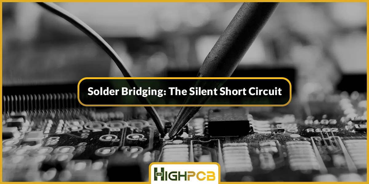
Solder Bridging: The Silent Short Circuit
Symptoms: Unintended electrical connections between adjacent pads or component leads.
Root Causes:
- Over-deposition of solder paste
- Inaccurate component placement
- Stencil design flaws
- Low-quality solder masks
Solutions:
- Refine stencil aperture designs, especially for fine-pitch components
- Employ solder mask-defined (SMD) pads where necessary
- Use under-stencil cleaning during long SMT runs
- Integrate automated optical inspection (AOI) at multiple stages
HighPCB’s Tip: Apply 3D SPI (Solder Paste Inspection) before reflow to identify paste volume inconsistencies.
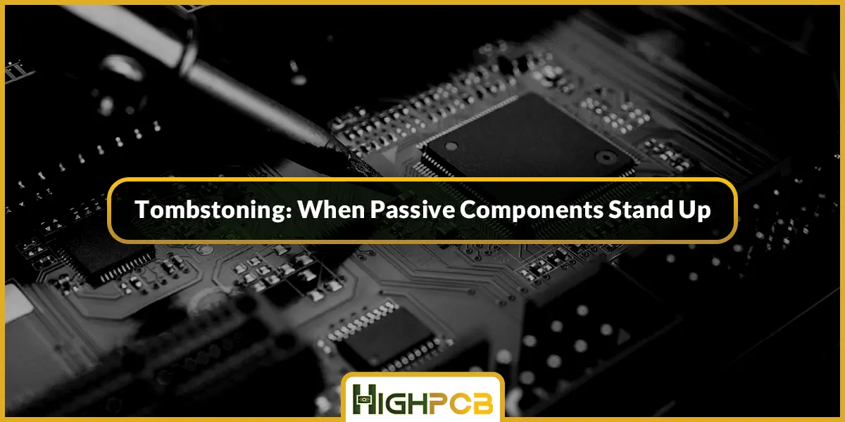
Tombstoning: When Passive Components Stand Up
Symptoms: One end of a passive chip (e.g., 0402 resistor) lifts up during reflow, forming an open circuit.
Root Causes:
- Asymmetrical heat transfer across component leads
- Disproportionate solder paste volume between pads
- High thermal gradient on the PCB surface
Solutions:
- Balance pad design to equalize thermal mass
- Apply consistent solder paste thickness using laser-cut stencils
- Optimize reflow profiles with a slow ramp rate to prevent thermal shock
HighPCB’s Tip: Run thermal simulations before finalizing layout, especially on high-density boards.
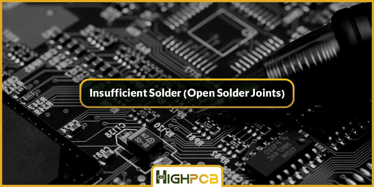
Insufficient Solder (Open Solder Joints)
Symptoms: Visibly small joints or open circuits, typically causing intermittent performance.
Root Causes:
- Low solder paste deposition
- Misaligned components
- Solder paste drying due to improper storage or handling
Solutions:
- Use humidity-controlled paste storage systems
- Perform regular stencil inspection and cleaning
- Improve pick-and-place accuracy through vision calibration
HighPCB’s Tip: Adopt a statistical process control (SPC) system to track paste volume consistency over time.
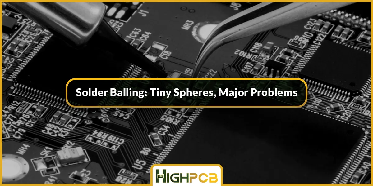
Solder Balling: Tiny Spheres, Major Problems
Symptoms: Small balls of solder scattered across the PCB surface, potentially leading to short circuits or cosmetic defects.
Root Causes:
- Aggressive flux chemistry
- Excessive solder paste volume
- Rapid temperature ramp-up
Solutions:
- Tune preheat zone in reflow ovens for a controlled temperature increase
- Use Type 4 or Type 5 solder paste for finer grain structure
- Clean PCBs and stencils with lint-free materials
HighPCB’s Tip: Use low-residue, halogen-free pastes to reduce post-reflow cleaning requirements.
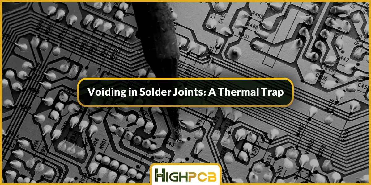
Voiding in Solder Joints: A Thermal Trap
Symptoms: Hidden air gaps inside solder joints, especially under large pads or thermal vias.
Root Causes:
- Entrapped volatiles during reflow
- Poor PCB via design
- Outgassing of inner PCB layers
Solutions:
- Apply vacuum reflow technology to reduce voids
- Design thermal vias with venting holes
- Use low-outgassing solder pastes
HighPCB’s Tip: Conduct X-ray inspection for all power and BGA components to detect internal voids.
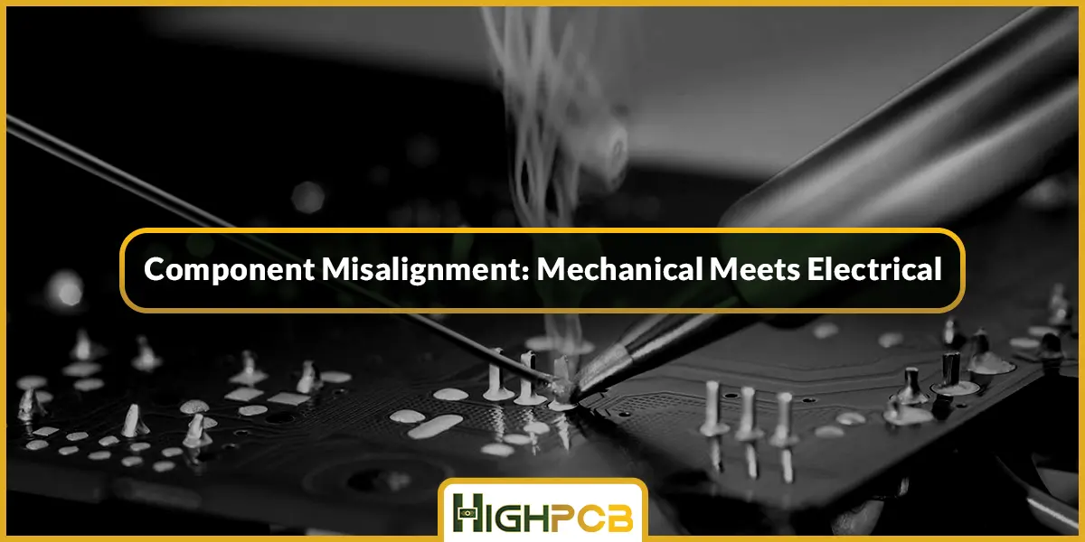
Component Misalignment: Mechanical Meets Electrical
Symptoms: Skewed or rotated components, leading to electrical faults or mechanical stress.
Root Causes:
- Vibrations during conveyor transitions
- Incorrect vacuum nozzle pressure
- Loss of solder paste tackiness
Solutions:
- Regularly calibrate pick-and-place machines
- Optimize placement force settings
- Store solder paste at manufacturer-recommended conditions
HighPCB’s Tip: Introduce fiducial marks and board supports to improve placement precision.
How HighPCB Ensures Soldering Excellence
At HighPCB, we integrate rigorous quality assurance at every stage:
- Advanced thermal profiling using real-time sensors
- Selective soldering for through-hole components
- X-ray and AOI inspections for critical assemblies
- Compliance with IPC-A-610, RoHS, and ISO 9001:2015
Our continuous improvement philosophy ensures that each solder joint meets or exceeds industry standards.
Conclusion: Build Reliability One Solder Joint at a Time
Solving soldering issues is more than troubleshooting—it’s about engineering for reliability. With a deep understanding of failure modes and process optimization, manufacturers can reduce costs, prevent recalls, and enhance their brand’s reputation.
HighPCB stands ready to help you diagnose, improve, and perfect your soldering processes—because quality starts at the smallest connection.