At HighPCB, we go beyond standard PCB fabrication by delivering precision, reliability, and flexibility tailored to your project’s needs. From multilayer and HDI boards to special laminates and high-frequency designs, our advanced capabilities ensure your products perform at the highest level.
With strict quality control, on-time delivery, and engineering support from prototyping to mass production, we help you reduce risks, speed up development, and achieve lasting reliability in every application.
Submit Yor PCB Fabrication Order!
HIGHPCB is a leading PCB manufacturing and PCB printing factory, delivering high-quality printed circuit boards (PCBs) for industries worldwide. With advanced PCB technology, precision engineering, and fast turnaround times, we provide reliable PCB solutions for prototypes, small batches, and mass production — ensuring durability, high performance, and cost-efficiency.
HIGHPCB – PCB Manufacturing And Printing Factory
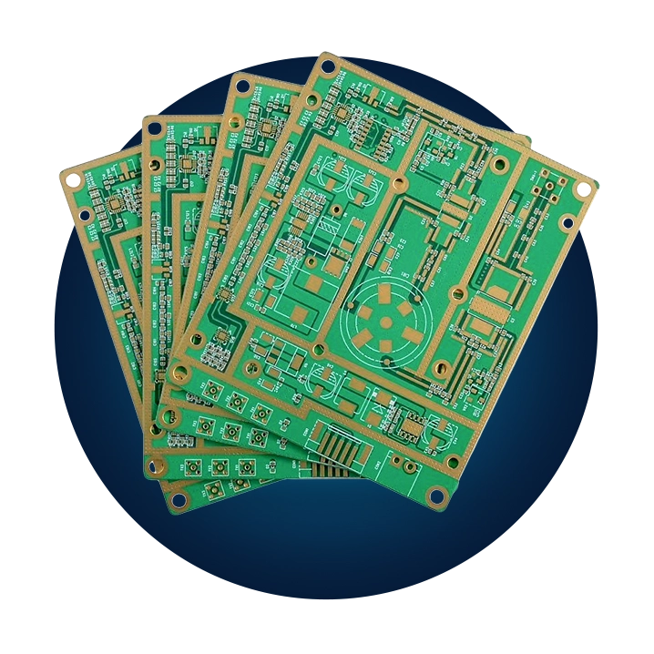
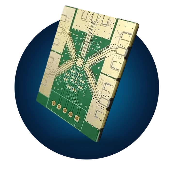
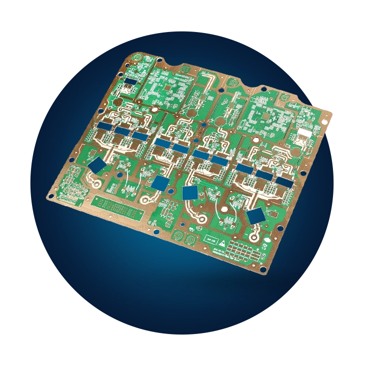
High Frequency PCB Fabrication at HIGHPCB delivers high-performance PCBs designed for RF and microwave applications. Using advanced materials, such as Rogers, Taconic, and other high-frequency laminates, we ensure low signal loss, high precision, and excellent reliability. Perfect for 5G, satellite communications, radar systems, and wireless devices, our high-frequency PCB solutions support both prototyping and mass production with strict quality control and fast turnaround times.
High Frequency PCB Fabrication
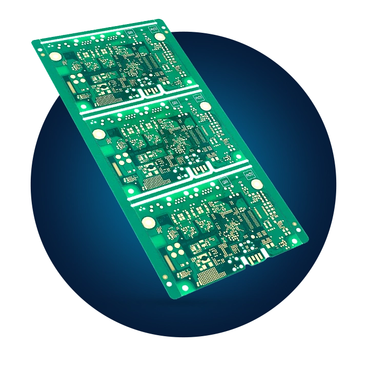
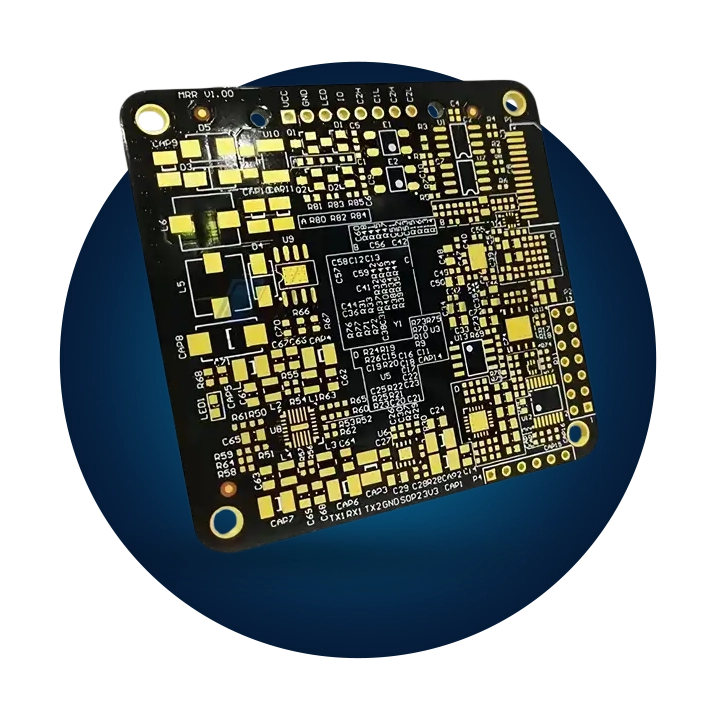
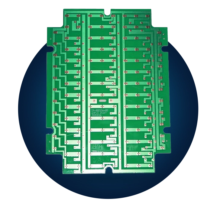
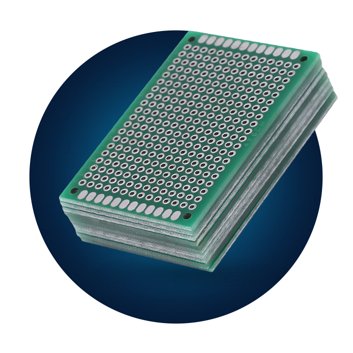
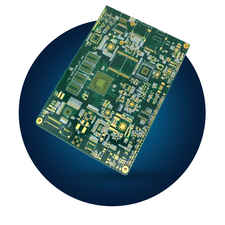
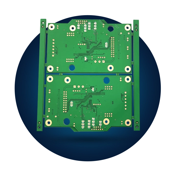
Rigid PCB Fabrication at HIGHPCB provides high-quality rigid PCBs for a wide range of industrial, automotive, consumer electronics, and medical applications. Our rigid circuit boards are built with advanced manufacturing technology to ensure durability, high performance, and long-term reliability. Whether you need single-layer, double-layer, or multilayer rigid PCBs, we deliver custom solutions with strict quality control, fast turnaround, and cost-effective pricing — from prototyping to mass production.
Rigid PCB Fabrication
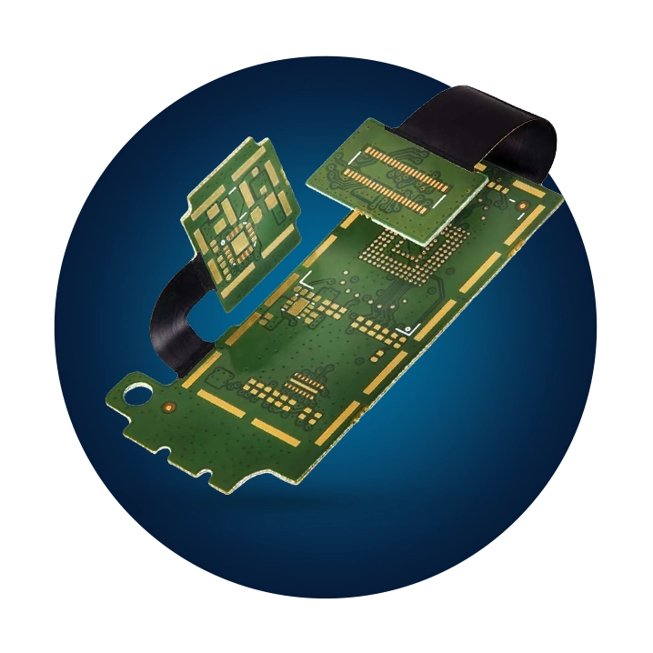
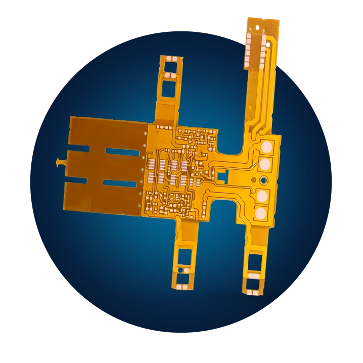
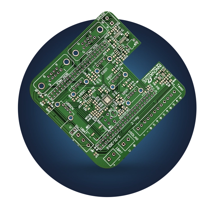
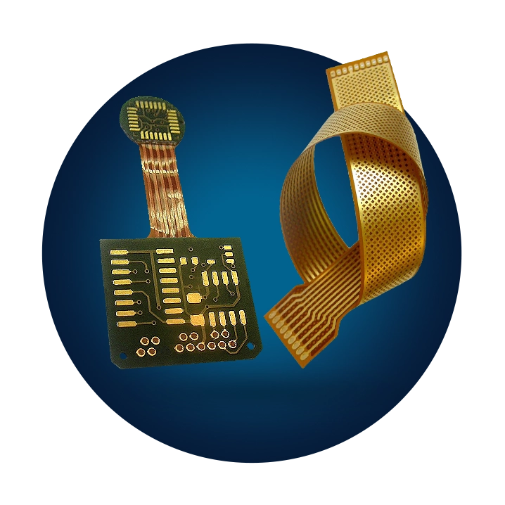
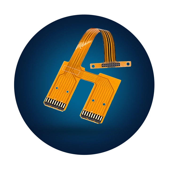
Flexible PCB Fabrication at HIGHPCB offers high-quality flexible PCBs designed for compact, lightweight, and dynamic electronic applications. Our flexible circuit boards deliver reliability, durability, and design versatility, making them ideal for wearable devices, medical equipment, automotive electronics, and aerospace systems. With advanced manufacturing technology, strict quality control, and fast turnaround times, we provide custom flexible PCB solutions for prototyping, small batches, and mass production — ensuring superior performance and cost-efficiency in every project.
Flexible PCB Fabrication
Why Choose HighPCB for Your PCB Fabrication?
At HighPCB, we focus on delivering high-quality, reliable, and cost-effective PCBs. Here’s a breakdown of our core capabilities:
Affordable Pricing
High-Quality Materials
Fast Turnaround Time
Expert Engineering Team
Customization
Comprehensive Quality Control
The PCB Fabrication Process
Understanding the fabrication process is crucial to selecting the right PCB for your project. Here’s a step-by-step breakdown of the typical PCB fabrication process:
1. Design and Prototyping:
The process begins with the creation of PCB design files (Gerber files) which detail the layout, components, and wiring of the circuit. During this phase, design is optimized for manufacturability.
2. Material Selection:
Based on the design requirements, the right material (rigid, flexible, aluminum, etc.) is chosen for the PCB.
3. Layer Formation and Etching:
For multi-layer boards, layers are stacked and etched to create the copper pathways that will form the circuit. Etching removes unwanted copper to leave the circuit design.
4. Drilling:
Holes are drilled into the PCB to allow for component placement and vias for electrical connections between layers.
5. Solder Mask and Silk Screen:
A solder mask is applied to protect the copper traces from external damage and to ensure proper soldering of components. Silk screening adds labels, logos, and part numbers to the board for ease of identification.
6. Final Testing and Inspection:
Each PCB undergoes electrical testing and visual inspections to ensure quality and functionality.
Choosing the Right PCB for Your Project
When selecting a PCB for your project, it’s important to consider the specific requirements of your design. The type of PCB you choose will depend on factors like:
Power Requirements:
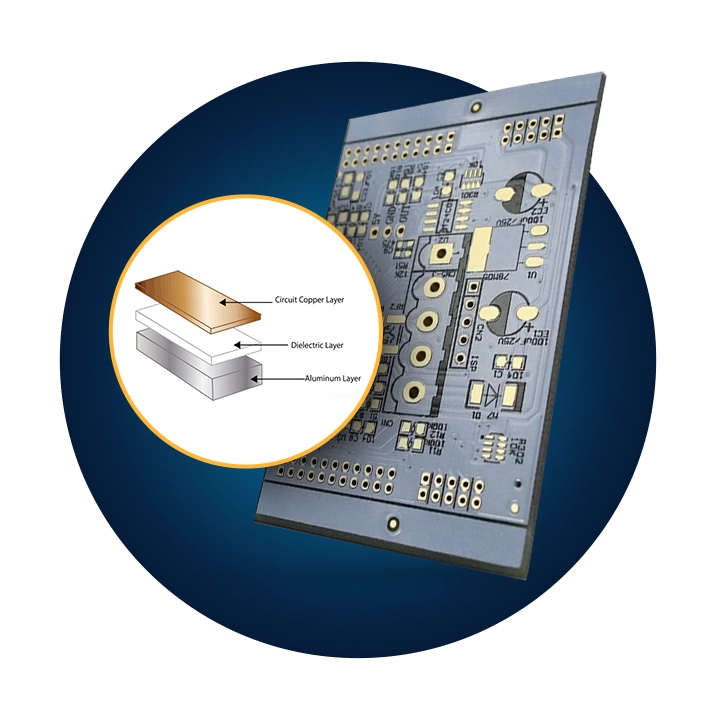
For high-power applications, consider Aluminum PCBs for better thermal management.
Space Constraints:
If your design needs to be compact and flexible, Flexible or Rigid-Flex PCBs might be the best option.
Signal Integrity:
For applications involving high-frequency signals, such as 5G or RF systems, High-Frequency PCBs are the ideal choice.
By carefully evaluating your needs and understanding the characteristics of each type of PCB, you can ensure that your design meets both functional and manufacturing requirements.
Get Started with HighPCB
We make the process easy:
1. Submit Your Design Files:
Send us your PCB design files to start the process.
2. Receive a Quick Quote:
We’ll provide a transparent quote based on your project requirements.
3. Approve the Design and Start Fabrication:
Once confirmed, we begin the fabrication process.
4. Delivery
Receive your high-quality PCBs on time, ready for assembly.


