


HighPCB is a specialist in high-frequency PCB fabrication for RF, microwave and 5G systems. We use advanced low-loss laminates such as Rogers RO4003C \ RO4350B and Taconic RF- 35, whose dielectric constants (~3.3 – 3.5) and very low dissipation factors (~0.002 – 0.003) minimize signal loss at 10 GHz. Our advantages include strict adherence to IPC-class workmanship, free DFx stack-up reviews, controlled-impedance coupons with test data, and fast prototype lead times to ensure first-pass success. With multilayer RF capabilities, various via and finish options (ENIG, immersion silver) and experience serving telecom, aerospace and medical customers, we provide reliable, high – performance boards tailored to your application.
HIGHPCB Advantages
Most experienced engineers
Free Design and Design Review
Most Strict quality control
Cost and time efficiency
High-end and quality equipment
All High frequency project types
Submit Yor High Frequency PCB Fabrication Order!
High Frequency PCB Fabrication Podcast

High Frequency PCB Fabrication Podcast - Episode 11
Listen to our latest tips for 2025, Powered By HIGHPCB.
Industry Standards We Build To
IPC-A-600 is the industry’s visual acceptance standard for bare PCBs. This standard clearly defines what is target, acceptable, or non-conforming for critical PCB features such as plating, voids, annular rings, solder mask, scratches, measling, and more. The requirements are organized by Class 1, Class 2, and Class 3 reliability levels, ensuring that manufacturers and inspectors can consistently evaluate PCB quality.
For RF and microwave PCB applications, IPC-A-600 remains the key reference for judging workmanship quality, and it is typically used alongside a performance specification such as IPC-6018 for high-frequency and microwave boards. This combination ensures both visual and functional quality standards are met, helping to guarantee reliability in advanced PCB applications.
IPC‑6018 – Qualification and Performance Specification for High-Frequency (Microwave) Printed Boards is the industry standard that defines the inspection, testing, and performance requirements for printed circuit boards (PCBs) used in microwave and RF applications. This standard applies to microstrip, stripline, and mixed-dielectric boards, including those with buried or blind vias and metal features.
The purpose of IPC‑6018 is to ensure the reliability of high-frequency boards by specifying qualification tests, end-product performance classes, and design-selection guidance. Following this standard helps manufacturers and engineers guarantee that microwave and RF PCBs meet strict performance and quality criteria, ensuring dependable operation in advanced electronic applications.
IPC‑4103 – Specification for Base Materials for High-Speed/High-Frequency Applications defines the requirements for clad and unclad plastic laminates and bonding materials used to fabricate high-speed and high-frequency printed circuit boards (PCBs). This standard allows the use of low-permittivity glass reinforcements to improve dielectric constant and loss tangent, ensuring that materials used in RF and microwave boards provide the low-loss characteristics needed for reliable high-frequency operation.
Following IPC‑4103 ensures that manufacturers select base materials that optimize signal integrity, minimize losses, and meet the stringent performance requirements of high-speed and microwave PCB applications. This standard is essential for engineers and designers working with RF, microwave, and high-frequency electronic systems.
IPC‑2141A – Design Guide for High-Speed Controlled-Impedance Circuit Boards serves as a comprehensive guide for circuit designers, packaging engineers, and PCB fabricators to understand when and how to implement controlled-impedance interconnects.
In high-speed digital and high-frequency analog circuits, the electrical properties of interconnections significantly affect performance. Using controlled impedance ensures that PCB traces remain within specified tolerances, preventing signal degradation and maintaining reliable operation.
The guide covers essential design principles, including line geometry, dielectric selection, and termination strategies, which are critical for achieving predictable impedance and low-loss characteristics in high-frequency PCBs. Following IPC‑2141A helps engineers and fabricators deliver high-performance PCB designs optimized for signal integrity and reliable high-speed operation.
Industry Standards We Build To
Use this quick selector to compare common RF laminates that we fabricate. The Dk (effective dielectric constant) impacts impedance and signal speed, while Df (dielectric loss) indicates loss characteristics—lower Df means less insertion loss.These values are typical and may vary depending on material thickness, copper weight, and test method, so they should be treated as guidance, not absolute values.Tell us your frequency band and stack-up goals, and our engineers will recommend the best RF laminate to ensure optimal performance in your high-frequency PCB designs.
| Material (Family) | Dk (10 GHz) | Df (10 GHz) | Tg (°C) | Td (°C) | Z-CTE (ppm/°C) | Surface Resist. (MΩ) | k (W/m·K) | Peel (N/mm) |
|---|---|---|---|---|---|---|---|---|
| Rogers RO4003C (hydrocarbon/ceramic) | 3.38 | 0.0027 | >280 | ~425 | ~46 | ~4.2×10⁹ | ~0.71 | ~1.05 |
| Rogers RO4350B (hydrocarbon/ceramic) | 3.48 | 0.0037 | >280 | ~390 | ~32 | ~5.7×10⁹ | ~0.69 | ~0.88 |
| Rogers RT/duroid 5870 (reinforced PTFE) | 2.33 | 0.0012 | — | ~500 | ~173 | ~2×10⁷ | ~0.22 | ~27.2 |
| Rogers RT/duroid 5880 (reinforced PTFE) | 2.20 | 0.0009 | — | ~500 | ~237 | ~3×10⁷ | ~0.32 | ~31.2 |
| Rogers RO3003 (ceramic-filled PTFE) | 3.00 | 0.0013 | — | ~500 | ~25 | ~1×10⁷ | ~0.50 | ~2.2 |
| Rogers RO3006 (ceramic-filled PTFE) | 6.2 | 0.0020 | — | ~500 | ~24 | ~1×10⁵ | ~0.79 | ~1.2 |
| Rogers RO3010 (ceramic-filled PTFE) | 10.0 | 0.0022 | — | ~500 | ~16 | ~1×10⁵ | ~0.95 | ~1.6 |
| Isola IS620 (E-glass) | ~4.5 | ~0.008 | ~220 | ~>300* | ~55* | ~2.8×10⁶* | — | ~1.2* |
| AGC Taconic RF-35 (ceramic) | ~3.5 | ~0.0018–0.002 | ~315 | ~>300* | ~64* | ~1.5×10⁸* | ~0.24* | ~1.8* |
| AGC Taconic TLX (PTFE) | 2.5 | ~0.0019 | — | ~135* | — | ~1×10⁷* | ~0.19* | ~2.1* |
| AGC Taconic TLC (PTFE) | 3.2 | — | — | ~70* | — | ~1×10⁷* | ~0.24* | ~2.1* |
| Arlon 85N (polyimide) | ~4.2 | ~0.010 | ~250 | ~387* | ~55* | ~1.6×10⁹* | ~0.20* | ~1.2* |

Where High-Frequency PCBs Are Used

5G & Telecom
Base-station antennas, small cells, RRUs, beam-forming arrays, LNAs/PAs, RF front-ends (sub-6 GHz & mmWave).
Aerospace & Defense
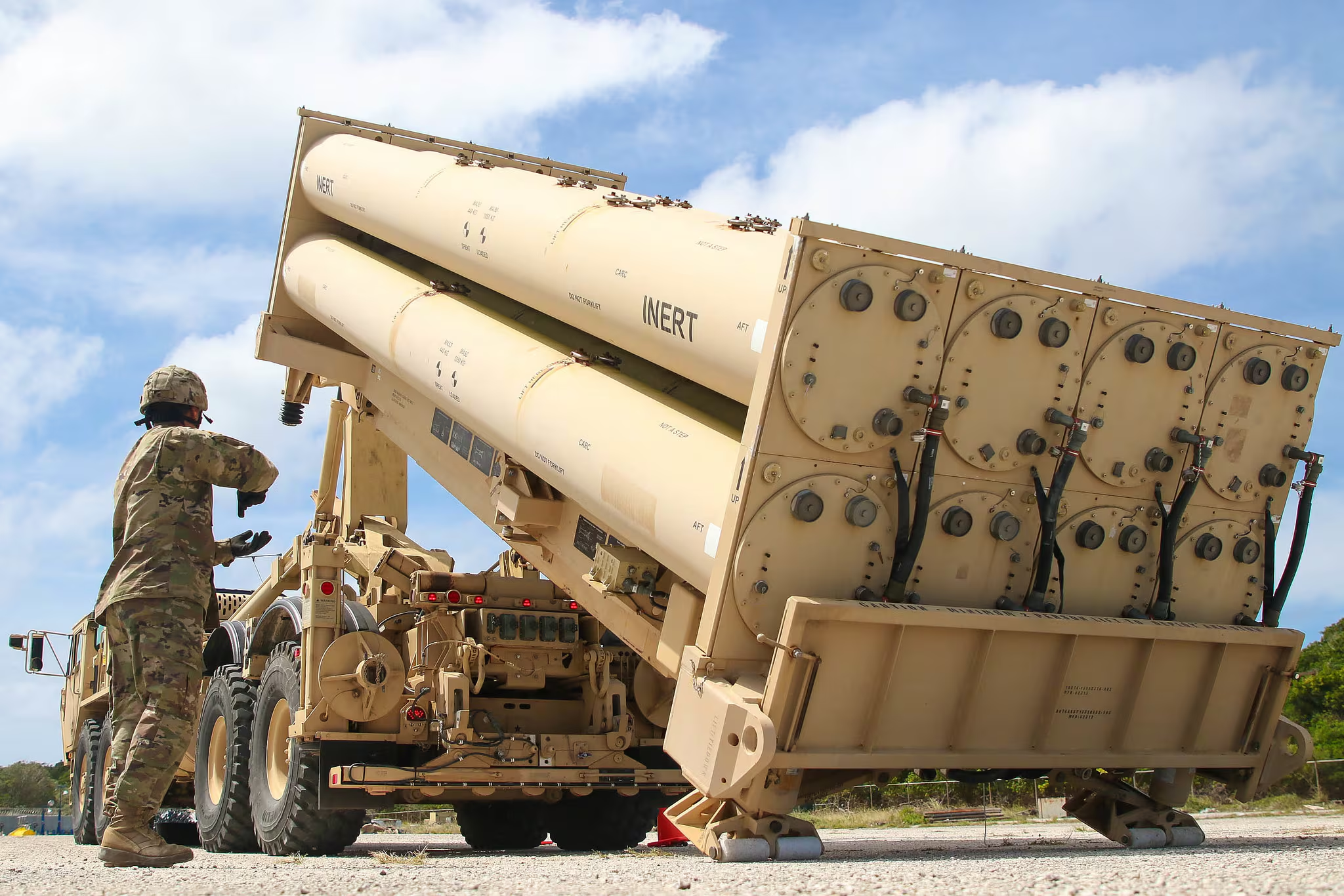
Radar (X/Ku/Ka-band), Sat-com transceivers, telemetry, EW/ELINT front-ends, phased arrays.

Automotive
24/77/79 GHz radar, V2X modules, GNSS receivers, high-precision positioning.

Medical & Life Sciences
Imaging coils and front-ends, patient telemetry, RF ablation drivers, wireless wearables.

Industrial & Test
Industrial & Test: Network analyzers, signal generators, NDT/ultrasonics drivers, RFID/UHF readers, UWB localization.

IoT & Consumer RF
Wi-Fi 6E/7 radios, Bluetooth/LE, UWB chips, GPS/GNSS, smart-home hubs and gateways.

Satellites & NewSpace
Satellites & NewSpace: Transponders, payload RF chains, TT&C, inter-satellite links.
High-Speed Digital / Mixed-Signal
SerDes breakouts, reference planes and controlled-impedance interconnects co-designed with RF sections.
Our capabilities
| Capability / Feature | Typical Range / Notes |
|---|---|
| Layer count | Standard: 1–16 layers; Advanced: up to 32 layers (some fabs support 40+ or “any layer” structures). |
| Board thickness | 0.4–4.5 mm overall. Common FR-4 options: 0.4/0.6/0.8/1.0/1.2/1.6/2.0 mm; 2.5 mm+ for 12-layer boards and above. Fineline’s R&D builds can go down to 0.20 mm. |
| Max/min board size | Standard: up to ~600 × 570 mm; Advanced: 960 × 600 mm; R&D: 1250 × 570 mm. Min board: 50 × 50 mm (standard), 30 × 30 mm (advanced), 5 × 5 mm (R&D). |
| Min trace/space | Standard: ~3 mil/3 mil (0.075 mm); Advanced: 2.5 mil/2.5 mil (0.063 mm); HDI/RF: 2 mil/2 mil (0.05 mm). HIGHPCB allows 0.10 mm on 1-oz copper, down to 0.09 mm on 4-layer boards. |
| Min via / drill diameters | Through-holes: 0.15–0.30 mm multilayer; 0.65 mm aluminium-core, 1 mm copper-core. Laser/microvia: 0.075 mm standard, 0.065 mm advanced. Min NPTH: 0.50 mm. |
| Aspect ratio (board thickness : hole diameter) | Standard 10:1, Advanced 16:1, R&D 20:1. |
| Copper weights | Outer layers: standard up to 3 oz; advanced up to 12 oz; R&D > 12 oz. Inner layers: similar. HIGHPCB: outer 1-2 oz, inner 0.5/1/2 oz. |
| Surface finish options | Standard: OSP, HASL, ENIG, immersion tin/silver; Advanced: adds hard gold, ENEPIG; High-end: ISIG, EPIG. HIGHPCB: HASL, ENIG, OSP. |
| Controlled impedance | Tolerance ±10%; High-end ±5% on request (many RF customers require this). |
| HDI / microvia support | Stacked/staggered microvias, copper-filled microvias, any-layer HDI on advanced lines. Laser via pads ~0.15 mm larger than via, shrinking to +0.10 mm on R&D. |
| Other clearances | Via-to-track ~0.20 mm; PTH-to-track recommended 0.35 mm (min 0.28 mm); NPTH-to-track 0.20 mm; same-net track 0.25 mm; inner-layer via-to-copper 0.20 mm. |
RF Design Rules
Best Practices for RF PCB Design: Ground Planes, Via Fences, and High-Speed Line Routing
-
Adjacent Ground Planes: Keep RF signals adjacent to a continuous ground plane. This confines electromagnetic fields and reduces unwanted radiation, improving overall signal integrity.
-
Dedicated RF Layers: Use one or more solid ground layers under RF traces. Avoid splitting the ground plane or routing signals between power and ground layers to minimize noise and coupling.
-
Via Fences: For grounded coplanar waveguides, place rows of ground vias on both sides of the signal line. This shorts loop currents to the underlying ground plane, maintaining consistent impedance and minimizing EMI.
-
Bend Radii: Always use a bend radius at least three times the line width to reduce impedance variations. If a right-angle bend is unavoidable, mitre the corner to preserve signal quality.
-
Layer Transitions: When a transmission line changes layers, use at least two vias. Pairing vias halves their inductive effect and ensures the finished via diameter matches the line width, reducing signal distortion.
-
Line Isolation: Keep RF lines spaced sufficiently apart to minimize coupling. Grounded coplanar waveguides offer good isolation, but achieving better than –45 dB isolation on a small PCB is challenging.
-
Separate RF, Digital, and Power Lines: Route high-speed digital lines on different layers from RF traces. Power lines should also be separated and properly decoupled to prevent interference.
-
Consistency with Stack-Up: Apply these rules according to your PCB laminate stack and ground-plane arrangement. Coplanar waveguide fences are less effective if the nearest reference plane is too far or split near the signal line.
-
Substrate and Frequency Considerations: The recommended bend radius (~3× line width) and line spacing assume typical RF laminates (Dk ≈3–4). For high frequencies or unusual substrates, refine these guidelines using impedance calculators or electromagnetic field solvers.
-
Return-Path Continuity: Paired vias not only reduce inductance but also maintain a continuous return path on the adjacent ground plane. Avoid routing high-speed lines over power-plane gaps or splits to uphold the “adjacent ground plane” principle.
-
Physical Separation of RF, Digital, and Power: Besides using separate layers, keep high-speed digital clocks and switching currents physically distant from RF circuitry. Use proper filtering on the power distribution network to minimize interference.
“Feel free to consult with our most experienced engineers about your design, or even let them design it for you.”
High-Frequency PCBs Explained
High-Frequency PCB Fabrication Process
Design & Prototyping
Create the PCB design based on electrical specifications and develop prototypes to validate the design.
Material Selection
Choose materials such as TACONIC or Rogers according to frequency range, loss requirements, and thermal stability.
Layer Formation
Stack multiple layers and apply circuit traces using etching and laser drilling for multilayer boards.
Drilling & Vias
Drill holes for component placement and vias to create proper electrical connections between layers.
Solder Mask & Surface Finish
Apply ENIG or Immersion Silver finishes to ensure solderability and reduce high-frequency losses.
Testing & Validation
Conduct impedance and RF performance testing to guarantee consistent electrical behavior.
Final QA & Documentation
Perform a final quality check and document design files, test results, and specifications for traceability.
Frequently Asked Questions (FAQ)
Frequently Asked Questions (RF PCB Fabrication)
Which RF materials do you support?
We stock hydrocarbon/ceramic laminates such as Rogers RO4003C and RO4350B (Dk ≈ 3.38–3.48 and Df ≈ 0.0027–0.0031), and Taconic RF‑35 variants (Dk ≈ 3.5 and Df ≈ 0.002 at 10 GHz). We choose materials based on your frequency range, loss budget, and thermal requirements.
What data formats do you accept?
We accept Gerber RS‑274X/X2, ODB++, and IPC‑2581. Native CAD files from Altium, KiCad, Eagle, etc., are also supported.
Can you provide impedance reports?
Yes. We include impedance coupons on the same panel as your board and measure them with calibrated fixtures. Reports show measured impedance vs target, and we can supply S-parameter measurements and TDR plots on request.
Which surface finish is best for high-frequency boards—ENIG or Immersion Silver?
ENIG provides a flat, durable surface and long shelf life, but the nickel layer can increase loss at very high frequencies.
Immersion Silver deposits a thin layer of pure silver, offering good conductivity and lower cost, but is less durable and must be soldered promptly.
ENEPIG is also available for bondable high-frequency applications.
Do you build hybrid stack-ups combining FR‑4 and RF cores?
Yes. For cost-sensitive designs including both high-speed digital and RF sections, we combine low-loss RF cores for critical layers with FR‑4 for other layers. We ensure transitions between materials do not introduce excess loss or impedance discontinuities.
What is your typical impedance tolerance?
Our standard controlled-impedance tolerance is ±5%, with tighter tolerances (±3%) available on request. Achieved through careful material selection, precise dielectric thickness control, and coupon-based verification.
How do via fences improve high-frequency performance?
Via fences are rows of ground vias on either side of a coplanar waveguide or board edge. They connect top-layer ground pours to a ground plane, confine loop currents, reduce signal leakage, and improve isolation between RF lines. In some microstrip or stripline designs, via fences also provide additional shielding.
